For configuration of the GPIO for SDHC peripheral usage see the General-Purpose I/O and Alternate Function Pins chapter.
8.5.2 SDHC Peripheral Clock Selection
The input clock to the SDHC peripheral is driven by the high speed system oscillator always, 96MHz. This 96MHz input clock
is either divided by 2 (default) or by 4 to drive the SDHC peripheral. Set the SDHC peripheral clock divisor using the
GCR_PCLK_DIV.sdhcfrq bit as shown
Equation 8-1: SDHC Peripheral Clock
8.5.3 Usage
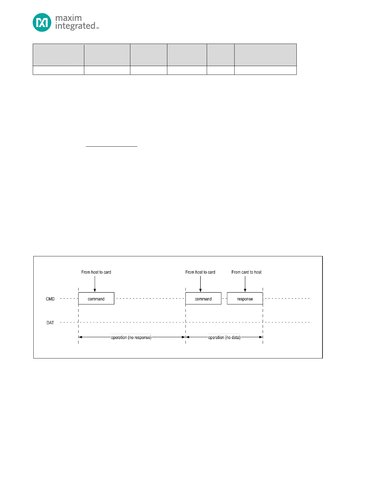
Communication over the SD bus is based on command and data bit streams/blocks that are initiated by a start bit and
terminated by a stop bit.
• Command: A command is a token that starts an operation and is sent by the SDHC to the card in the embedded
card slot. A command is transferred serially using the SDHC_CMD pin.
• Response: A response is a token sent from the card to the SDHC in response to a previously received command
and is transferred serially using the SDHC_CMD pin.
• Data: You can transfer data from the card to the SDHC or vice versa using the SDHC_DAT[3:0] pins.
Figure 8-8, Figure 8-9, and Figure 8-10 show the basic types of SD operations as described in the Physical Layer Simplified
Specification Version 6.00 from the SD Card Association.
Figure 8-8: SD Bus Protocol - No Response and No Data Operations