MAX32665-MAX32668 User Guide
Maxim Integrated Page 67 of 457
4.8 RAM Memory Management
This device has many features for managing the on-chip RAM. The on-chip RAM includes data RAM, instruction and data
caches, and peripheral FIFOs.
4.8.1 RAM Zeroization
The GCR Memory Zeroize Register, GCR_MEM_ZERO, allows clearing memory for firmware or security reasons. Zeroization
writes all zeros to the specified memory.
The following RAM memories can be zeroized:
• The Internal Data RAMs 0 through 6.
Each of the internal data RAM segments can be zeroized independently by setting the
GCR_MEM_ZERO.sram0z through GCR_MEM_ZERO.sram6z fields to 1.
• The USB FIFO
Write 1 to GCR_MEM_ZERO.usbfifoz
• ICC0 16KB Cache
Write 1 to GCR_MEM_ZERO.icache0z
• ICC1 16KB Cache
Write 1 to GCR_MEM_ZERO.icache1z
• SRCC Cache Tags
Write 1 to GCR_MEM_ZERO.scachetagz
This clears the Cache tags, ultimately invalidating the SRCC cache memory as well.
• SRCC 16KB Cache Data
Write 1 to GCR_MEM_ZERO.scachedataz
• SFCC 16KB Cache
Write 1 to GCR_MEM_ZERO.icachexipz
• Crypto MAA RAM (MAX32666/MAX32668)
Write 1 to GCR_MEM_ZERO.cryptoz
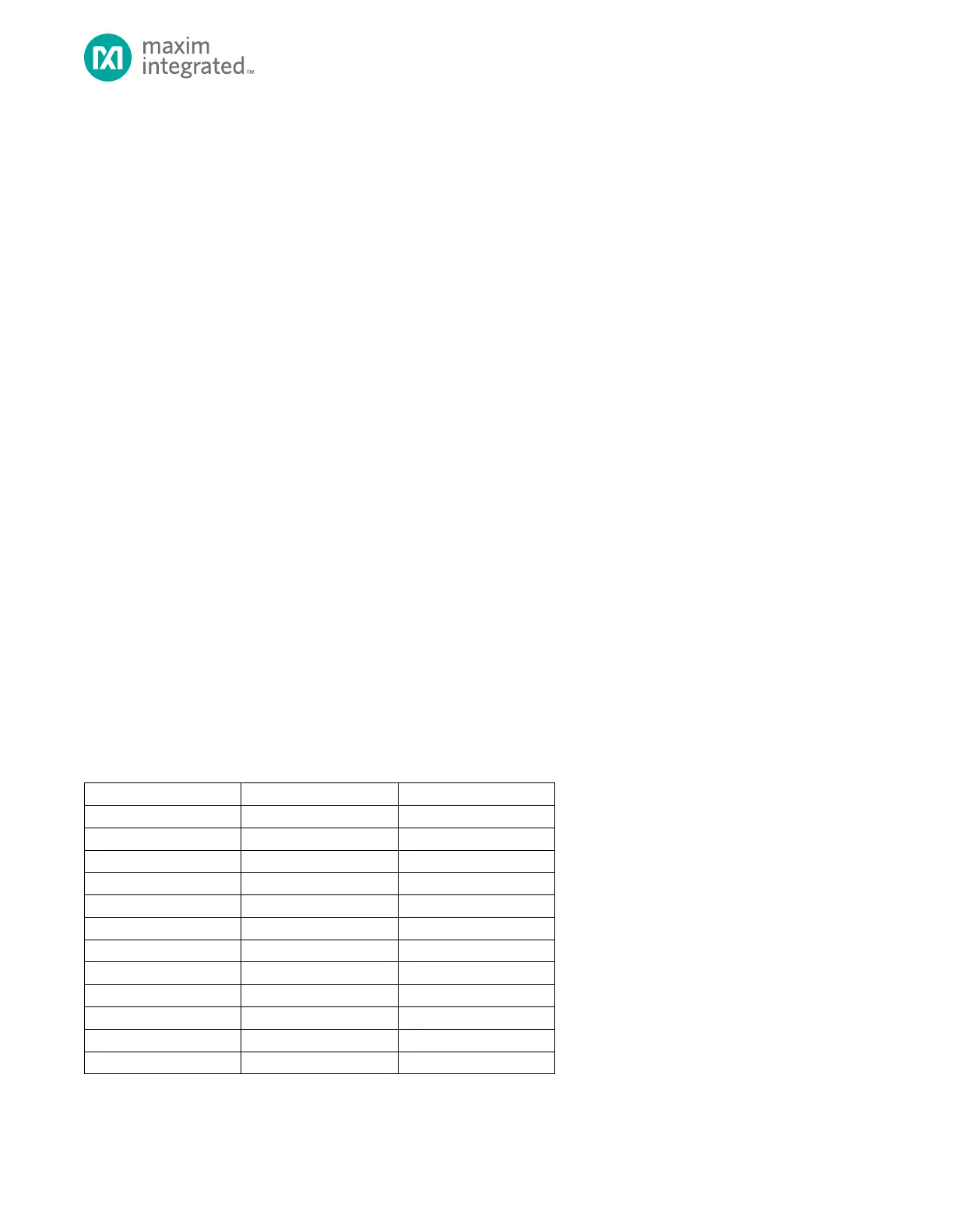
4.8.2 RAM Low Power Modes
RAM low power modes and shutdown are controlled on a bank basis. The System RAM banks are shown with
corresponding bank sizes and base addresses in below:
Table 4-13 RAM Block Size and Base Address