MAX32665-MAX32668 User Guide
Maxim Integrated Page 311 of 457
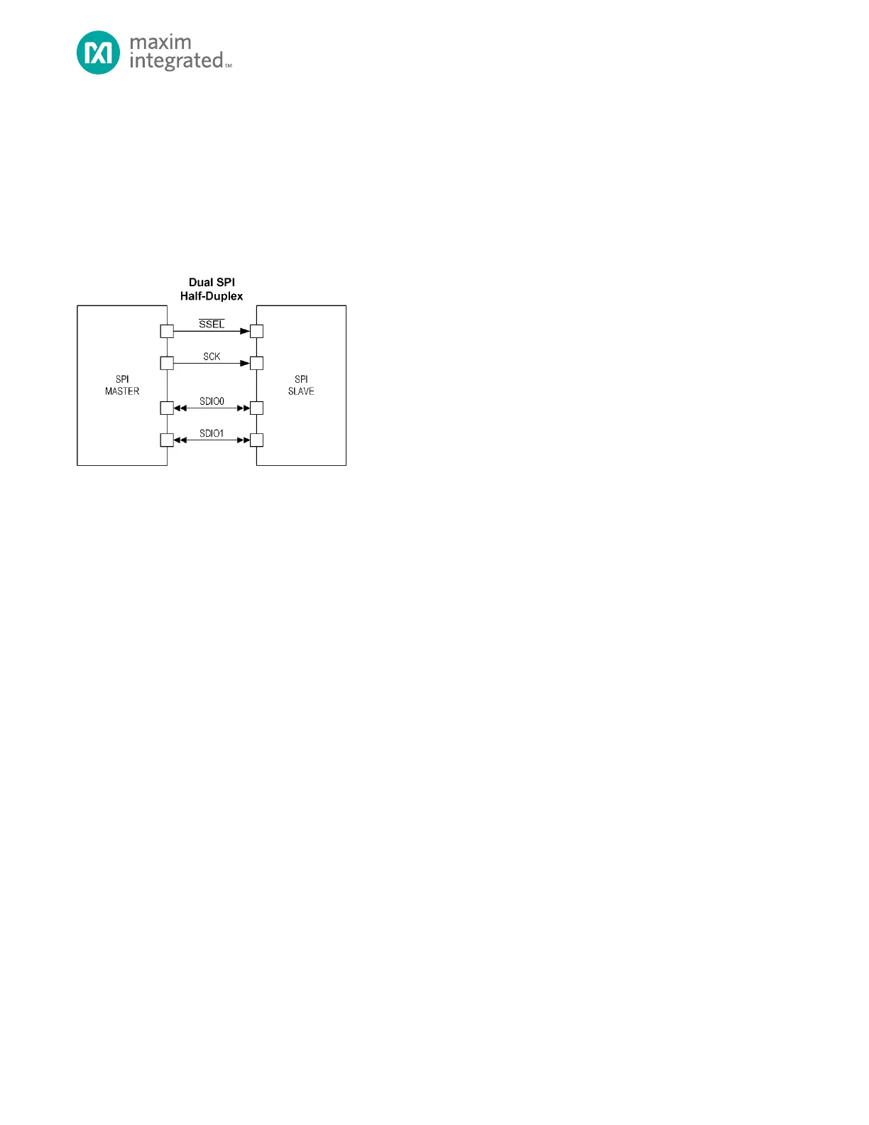
14.3.4 Dual Mode Format Configuration
In Dual mode SPI two I/O pins are used to transmit 2-bits of data per SCK clock cycle. The communication is half-duplex and
the direction of the data transmission must be known by both the master and slave for a given transaction. Dual mode SPI
uses SCK, SDIO0, SDIO1 and one or more slave select lines as shown in Figure 14-4, below. The configuration of the GPIO
pins for Dual mode SPI is identical to four wire SPI and the mode is controlled by setting QSPIn_CTRL2.data_width to 1
indicating to the QSPIn hardware to use SDIO0 and SDIO1 for half-duplex communication rather than full-duplex
communication.
Figure 14-4: Dual Mode SPI Connection Diagram
14.3.5 Quad Mode Format Pin Configuration
Quad mode SPI uses four I/O pins to transmit four-bits of data per transaction. In Quad mode SPI, the communication is
half-duplex and the master and slave must know the direction of transmission for each transaction. Quad mode SPI uses
SCK, SDIO0, SDIO1, SDIO2, SDIO3 and one or more slave select pins.
Quad mode SPI transmits four bits per SCK cycle. Selection of Quad mode SPI is selected by setting
QSPIn_CTRL2.data_width to 2.
14.4 QSPI Clock Configuration
14.4.1 Serial Clock
The SCK signal synchronizes data movement in and out of the device. The master drives SCK as an output to the slave’s SCK
pin. When QSPIn is set to master mode, the QSPIn bit rate generator creates the serial clock and outputs it on the
configured QSPIn_SCK pin. When QSPIn is configured for slave operation the QSPIn_SCK pin is an input from the external
master and the QSPIn hardware synchronizes communications using the SCK input. Operating as a slave, if a QSPIn slave
select input is not asserted, the QSPIn ignores any signals on the serial clock and serial data lines.
When QSPIn is configured for slave operation, the maximum SCK input frequency supported is
. For example,
if
, the maximum SPI clock frequency supported in slave mode for QSPIn is 6MHz.
In both master and slave devices, data is shifted on one edge of the SCK and is sampled on the opposite edge where data is
stable. Data availability and sampling time is controlled using the SPI phase control field, QSPIn_CTRL2.phase. The SCK clock
polarity field, QSPIn_CTRL2.clkpol, controls if the SCK signal is active high or active low.
The QSPIn peripheral supports four combinations of SCK phase and polarity referred to as SPI Modes 0, 1, 2, and 3. Clock
Polarity (QSPIn_CTRL2.clkpol) selects an active low/high clock and has no effect on the transfer format. Clock Phase
(QSPIn_CTRL2.phase) selects one of two different transfer formats.
For proper data transmission, the clock phase and polarity must be identical for the SPI master and slave. The master
always places data on the MOSI line a half-cycle before the SCK edge for the slave to latch the data. See section Clock Phase
and Polarity Control for additional details.