MAX32665-MAX32668 User Guide
Maxim Integrated Page 151 of 457
8.2.1.2 SPIXF Master Controller Registers
See Table 3-1: APB Peripheral Base Address Map for the SPIXF Peripheral Base Offset Address.
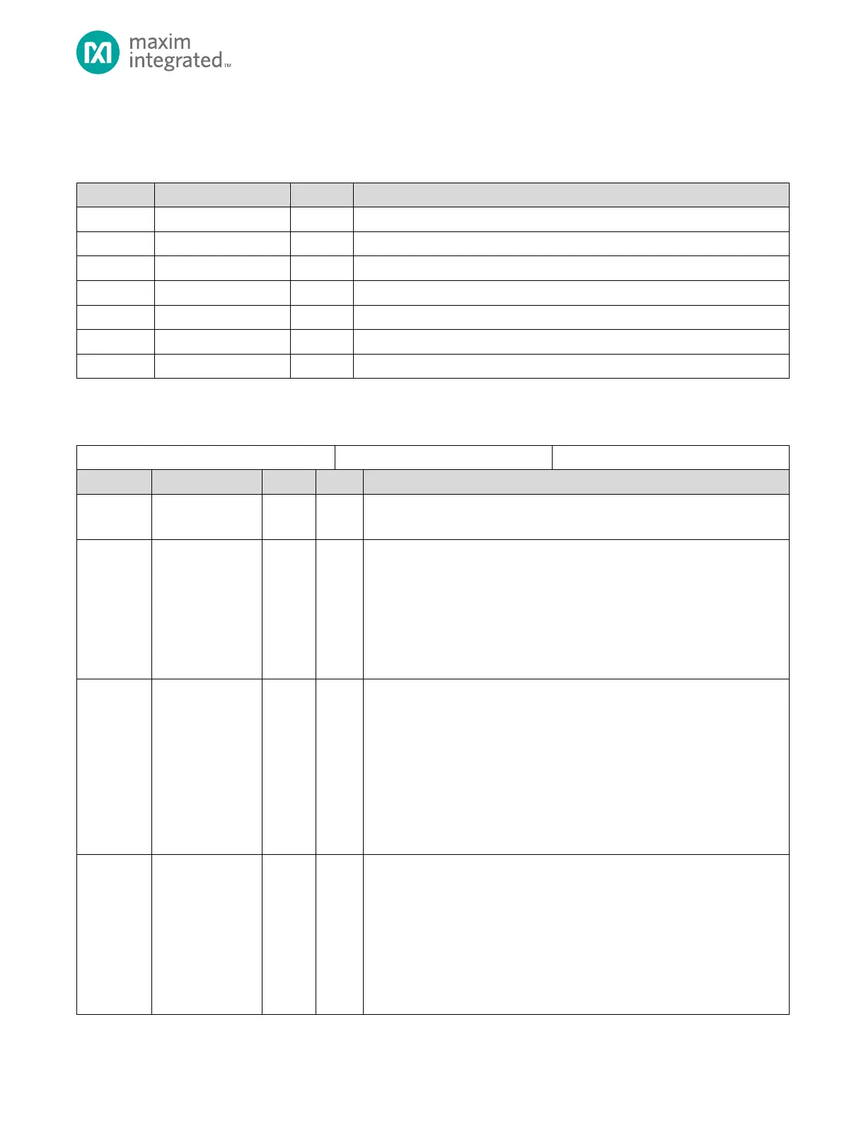
Table 8-4. SPIXF Master Controller Register Offsets, Names, Access and Description
SPIXF Controller Configuration Register
SPIXF Controller Slave Select Polarity Register
SPIXF Controller General Controller Register
SPIXF Controller FIFO Control and Status Register
SPIXF Controller Special Control Register
SPIXF Controller Interrupt Status Register
SPIXF Controller Interrupt Enable Register
8.2.1.3 SPIXF Master Controller Register Details
Table 8-5. SPIXF Controller Configuration Register
SPIXF Controller Configuration Register
Reserved for Future Use
Do not modify this field.
Sample Delay
Defines additional delay in SPI clock periods to wait before sampling SDIO input.
This value must be less than or equal to the value set for HICLK (for SPI modes 0
and 3). This value applies only in non-clock feedback mode
(SPIXFC_GEN_CTRL.sckfb = 0).
0b0000: No Delay
0b0001: 1 SPI Clock delay
0b1111: 15 SPI Clock delay
Slave Select Inactive Stretch
This field controls the number of system clocks the bus is inactive between the
end of a transaction (Slave Select inactive) and the start of the next transaction
(Slave Select active).
See section Slave Select Transaction Delay Configuration for detailed
information.
0b00: 4 system clocks
0b01: 6 system clocks
0b10: 8 system clocks
0b11: 12 system clocks
Slave Select Holdoff
Controls the delay from assertion of slave select to the start of SCK pulse and the
delay from the end of SCK pulses to de-assertion of slave select.
See section Slave Select Transaction Delay Configuration for detailed
information.
0b00: 0 system clocks
0b01: 2 system clocks
0b10: 4 system clocks
0b11: 8 system clocks