MAX32665-MAX32668 User Guide
Maxim Integrated Page 279 of 457
Equation 13-4: I
2
C Peripheral Source Clock Period
t
I2CCLK
2
f
SYSCLK
0
73728MHz1
In Hs-mode, the analog glitch filter within the device adds a minimum delay of t
AF_MIN
= 10ns.
Equation 13-5: Determining the I2Cn_HS_CLK .hs_clk_lo Register Value
t
LOWMIN
t
t
I2CCLK
t
t
I2CCLK
Equation 13-6: Determining the I2Cn_HS_CLK .hs_clk_hi Register Value
t
HIGHMIN
t
rCLMAX
t
I2CCLK
t
AFMIN
t
I2CCLK
-1
Equation 13-7: The Calculated Frequency of the I
2
C Bus Clock Using the Results of Equation 13-5 and Equation 13-6
CalculatedFrequency
1
1
t
I2CCLK
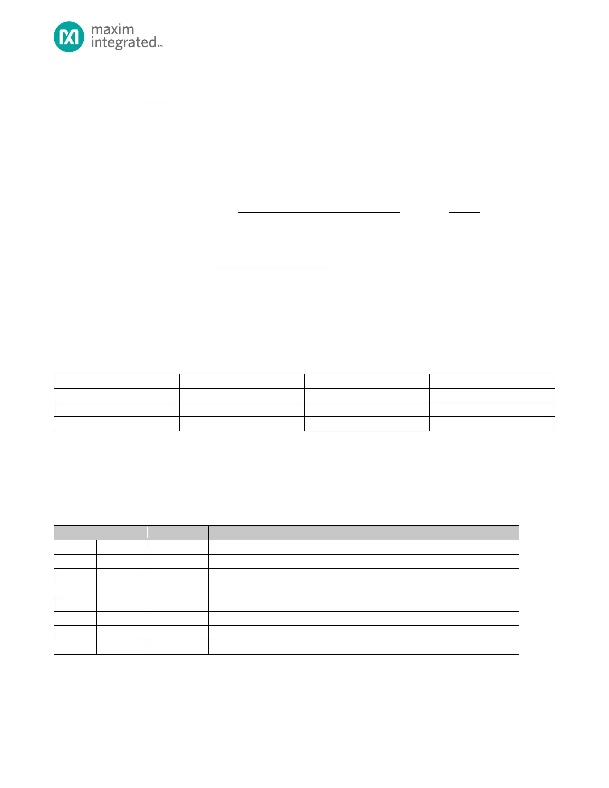
Table 13-3: Calculated I2C Bus Clock Frequencies shows the I
2
C bus clock calculated frequencies given different f
sys_clk
frequencies.
Table 13-3: Calculated I
2
C Bus Clock Frequencies
Calculated Frequency (MHz)
13.4.5 I
2
C Addressing
After a START condition, an I
2
C slave address byte is transmitted. The I
2
C slave address is composed of a slave address
followed by a read/write bit.
Table 13-4: I
2
C Slave Address Format
Reserved for different bus format
Reserved for future purposes
Reserved for future purposes