MAX32665-MAX32668 User Guide
Maxim Integrated Page 149 of 457
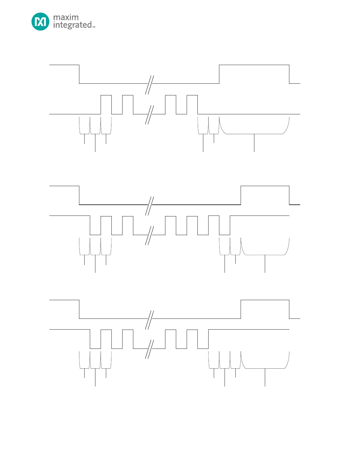
Figure 8-3. SPIXFC Transaction Delay
SPIXFC MODE 0
SPIXFC_CFG.ssact
SPIXFC_CFG.loclk
SPIXFC_CFG.hiclk
SS
SCK
SPIXFC_CFG.loclk
SPIXFC_CFG.ssact
SPIXFC_CFG.inact
SPIXFC_CFG.ssact
SPIXFC_CFG.loclk
SPIXFC_CFG.hiclk
SS
SCK
SPIXFC_CFG.loclk
SPIXFC_CFG.ssact
SPIXFC_CFG.inact
Bit 0
Extra
Pulse
SPIXFC MODE 3, SPIXFC_SP_CTRL.sckinh3 = 0
SPIXFC_CFG.ssact
SPIXFC_CFG.loclk
SPIXFC_CFG.hiclk
SS
SCK
SPIXFC_CFG.loclk
SPIXFC_CFG.ssact
SPIXFC_CFG.inact
Bit 0
SPIXFC MODE 3, SPIXFC_SP_CTRL.sckinh3 = 1
SPIXFC_CFG.hiclk
An extra pulse is provided at the end of this transaction to
comply with some SPI f lash timing diagrams, and allow for
higher speeds during SPI READ transa ctions. SCKINH3 =
0 should not be used for SPI WRITE transactions.
When sendin g a SPI WRITE transaction in MODE 3,
SCKINH3 should always be set in order to provide the
correct number of clocks.