MAX32665-MAX32668 User Guide
Maxim Integrated Page 162 of 457
SPIXFM slave select is low, the user must not be executing from SPIXFM space, and the SPIXF block should be reset by
setting GCR_RST1.spixip = 1.
8.2.2.7 External SPI Flash Decryption
If data in the SPI flash is encrypted when written, it might be transparently decrypted on read back using either code
execution or data reads. Decryption is not enabled by default. Setting SPIXFM_SEC_CTRL.dec_en = 1 enables the Memory
Decryption Integrity Unit (MDIU). The MDIU uses an AES-128 algorithm in ECB mode. This key is written by the user to the
register file locations 0x4000 5020 to 0x4000 502F, which is automatically used by the MDIU for decryption.
See SPIXF Master Controller for information about data encryption for external SPI flash.
8.2.2.8 SPIXFM Master Registers
See Table 3-1: APB Peripheral Base Address Map for the SPIXFM Master Peripheral Base Offset Address.
Reserved register bits should only be written as 0.
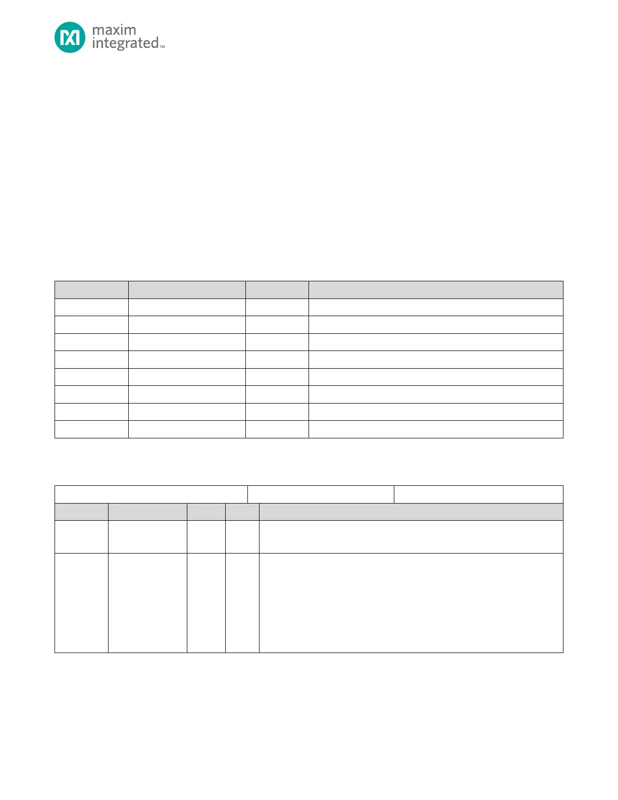
Table 8-15. SPIXFM Master Register Offsets, Names, Access and Description
Slave Select Inactive Timing
Controls delay from de-assertion of slave select to re-assertion of slave select for
another SPI transaction. See 8.2.1.1.6, above, for details on slave select
transaction delay configuration.
0b00: 1 system clocks
0b01: 3 system clocks
0b10: 5 system clocks
0b11: 9 system clocks