MAX32665-MAX32668 User Guide
Maxim Integrated Page 33 of 457
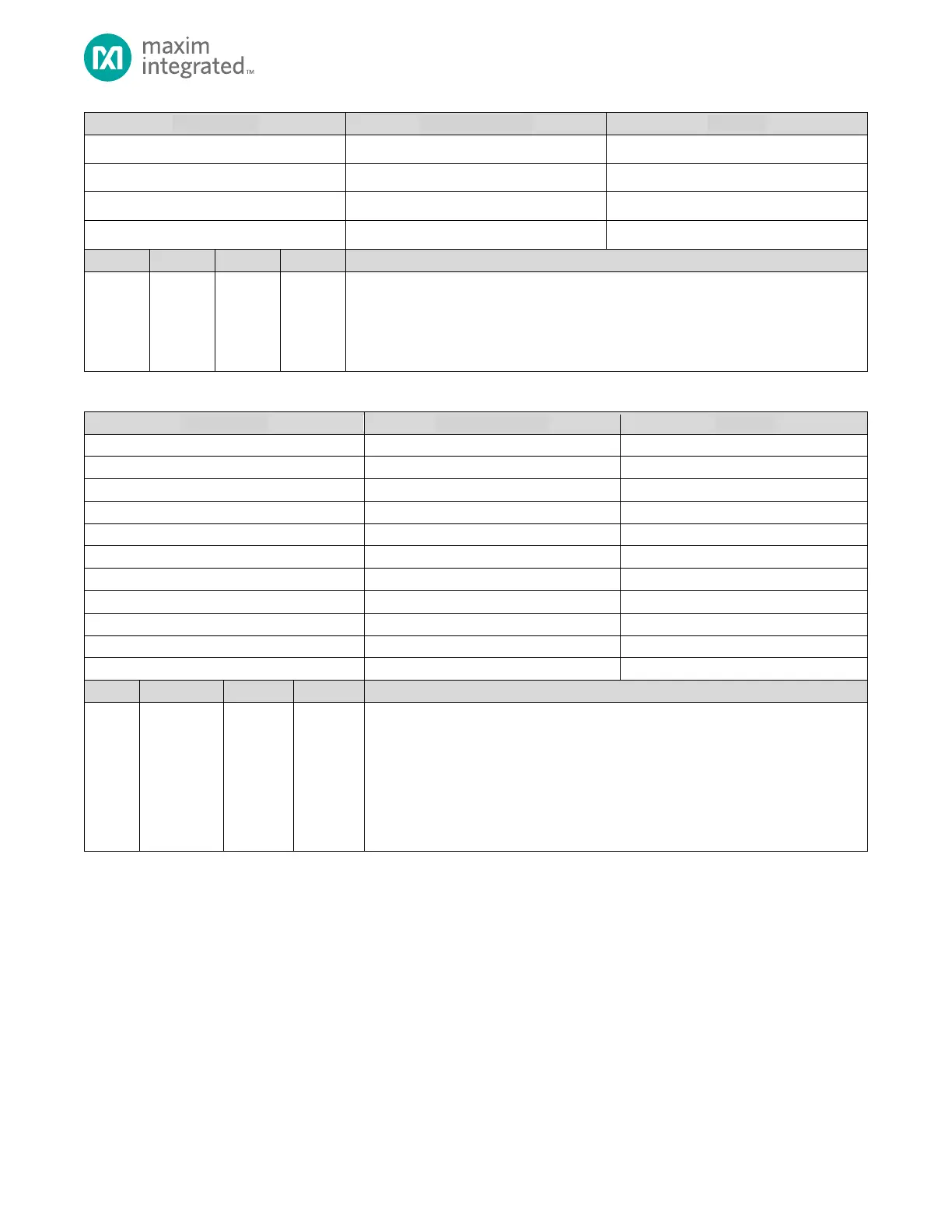
I2C 0 (Bus 1) RPU Register
I2C 1 (Bus 1) RPU Register
I2C 2 (Bus 1) RPU Register
Pulse Train Engine (Bus 1) RPU Register
APB Slave Peripheral Access Disable
0: AHB master read/write access allowed
1: AHB master read/write access denied
This field allows or denies access to the peripheral by one or more AHB masters as shown
in Table 2-2. Unused bits should not be changed from their reset default values
Table 2-8: RPU AHB Slave Permission Register
USB Endpoint Data RPU Register
SDIO/SDHC Target Memory RPU Register
SPI Bus Master FIFO RPU Register
QSPI Data Buffer RPU Register
System RAM, Memory Instance 0
System RAM, Memory Instance 1
System RAM, Memory Instance 2
System RAM, Memory Instance 3
System RAM, Memory Instance 4
System RAM, Memory Instance 5
System RAM, Memory Instance 6
AHB Slave Peripheral Access Disable
0b00: AHB master write/read access allowed
0b01: AHB master write access allowed / read access denied
0b10: AHB master write access denied / read access allowed
0b11: AHB master write/read access denied
Each bit pair of this field allows or denies access to the peripheral by one or more AHB
masters as shown in Table 2-2. Unused bits should not be changed from their reset
default values.