MAX32665-MAX32668 User Guide
Maxim Integrated Page 96 of 457
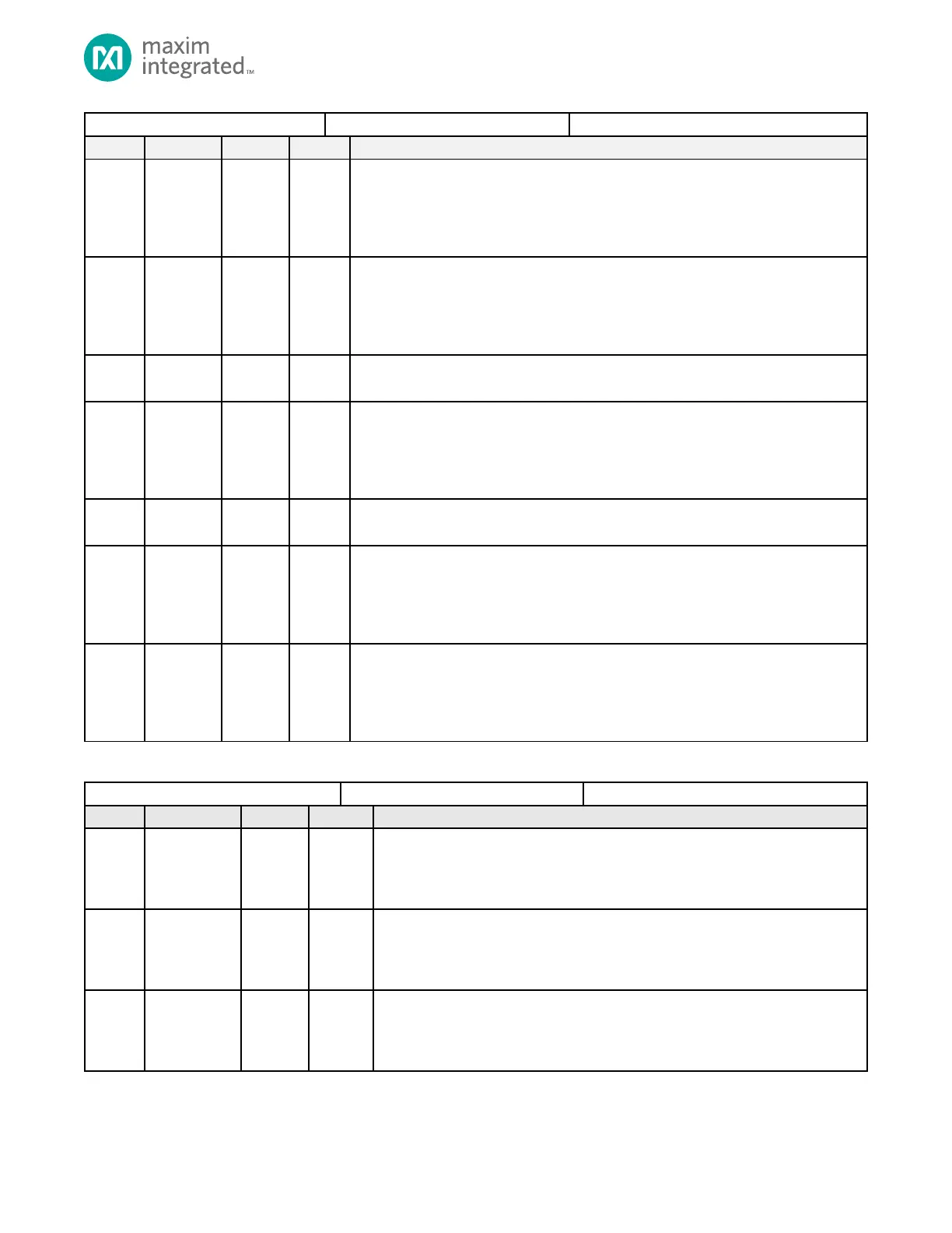
Peripheral Clocks Disable 0
SPI0 Clock Disable
Disabling a clock disables functionality while also saving power. Reads and writes to
peripheral registers are disabled. Peripheral register states are retained.
0: Clock enabled.
1: Clock disabled.
DMA0 Clock Disable
Disabling a clock disables functionality while also saving power. Reads and writes to
peripheral registers are disabled. Peripheral register states are retained.
0: Clock enabled.
1: Clock disabled.
Reserved
Do not modify this field.
USB Clock Disable
Disabling a clock disables functionality while also saving power. Reads and writes to
peripheral registers are disabled. Peripheral register states are retained.
0: Clock enabled.
1: Clock disabled.
Reserved
Do not modify this field.
GPIO1 Port and Pad Logic Clock Disable
Disabling a clock disables functionality while also saving power. Reads and writes to
peripheral registers are disabled. Peripheral register states are retained.
0: Clock enabled.
1: Clock disabled.
GPIO0 Port and Pad Logic Clock Disable
Disabling a clock disables functionality while also saving power. Reads and writes to
peripheral registers are disabled. Peripheral register states are retained.
0: Clock enabled.
1: Clock disabled.
Table 4-60: Memory Clock Control Register
Internal Flash ICC1 LIGHTSLEEP Enable
Data is unavailable for read/write operations in LIGHTSLEEP mode but is retained.
0: ACTIVE mode.
1: LIGHTSLEEP mode enabled.
ROM1 LIGHTSLEEP Enable
Data is unavailable for read/write operations in LIGHTSLEEP mode but is retained.
0: ACTIVE mode.
1: LIGHTSLEEP mode enabled.
ROM0 LIGHTSLEEP Enable
Data is unavailable for read/write operations in LIGHTSLEEP mode but is retained.
0: ACTIVE mode.
1: LIGHTSLEEP mode enabled.