MAX32665-MAX32668 User Guide
Maxim Integrated Page 74 of 457
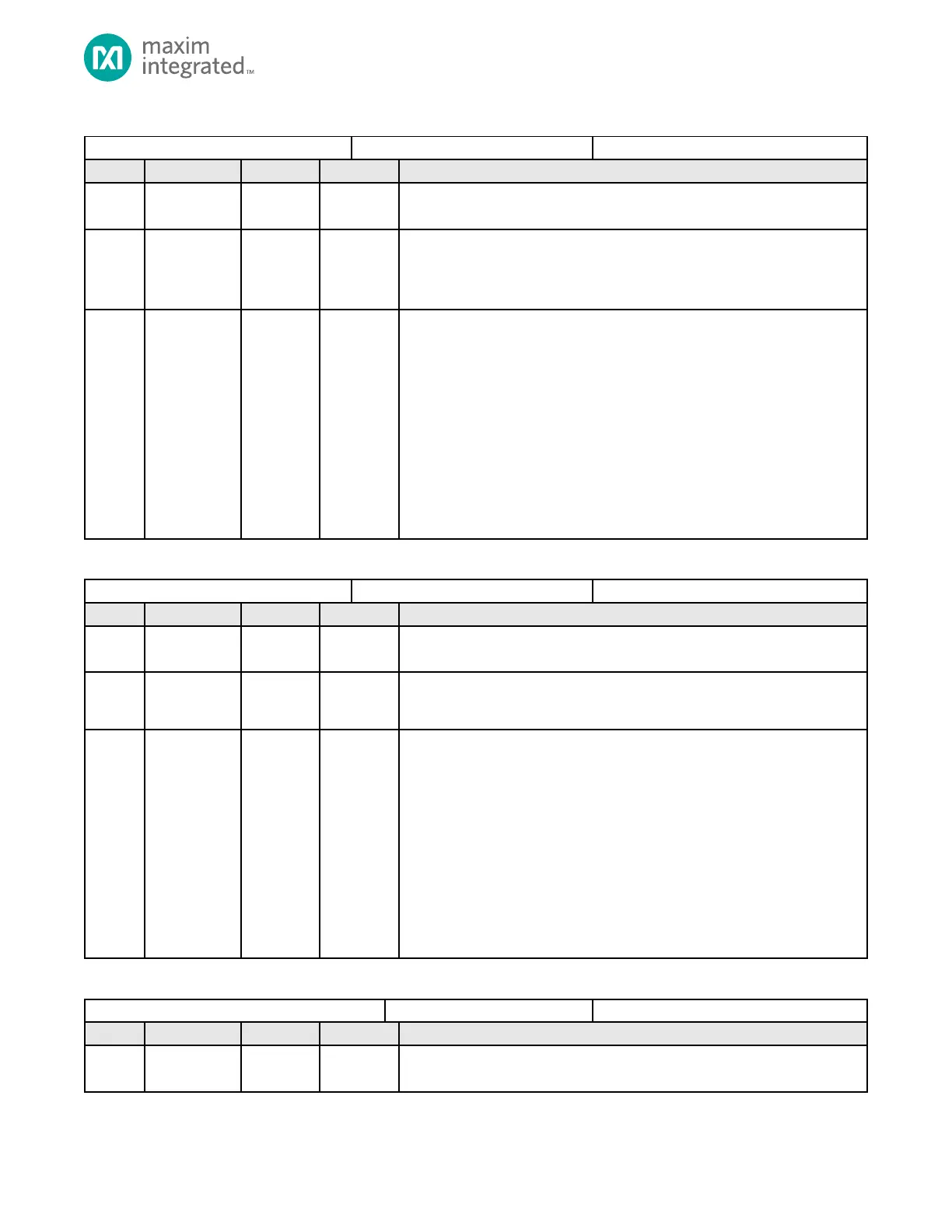
Table 4-23: Buck Voltage Regulator C Control Register
Buck Voltage Regulator A Control
Reserved
Do not modify this field.
Regulator Output Range
The voltage regulator output range setting.
0: 0.5V to 1.77
1: 0.6V to 1.87V
Regulator Output Voltage
Each increment in the register represents 10mV.
rangec = 1;
rangec = 0;
0x7Fh: 1.77V when rangec = 0; 1.87V when rangec = 1
Default: 0x32h = 1.0V when rangec = 0; 1.1V when rangec = 1
Warning: When this regulator is connected as shown in SIMO Power
Supply Device Pin Connectivity:
A: The maximum setting for this regulator must be followed for V
COREA
as
indicated in the device datasheet.
B: Setting the regulator to a voltage below the Power-Fail Reset Voltage
for V
COREA
will initiate the Power Monitor Reset Action.
Table 4-24: Buck Voltage Regulator D Control Register
Buck Voltage Regulator D Control
Reserved
Do not modify this field.
Regulator Output Range
0: 0.5V to 1.77
1: 0.6V to 1.87V
Regulator Output Voltage
Each increment in the register represents 10mV.
ranged = 1;
ranged = 0;
0x7Fh: 1.77V when ranged = 0; 1.87V when ranged = 1
Default: 0x32h = 1.0V when ranged = 0; 1.1V when ranged = 1
Warning: When this regulator is connected as shown in SIMO Power
Supply Device Pin Connectivity:
A: The maximum setting for this regulator must be followed for V
RXIN
and
V
TXIN
as indicated in the device datasheet.
B: Setting the regulator to a voltage below the Power-Fail Reset Voltage
for V
RXIN
and/or V
TXIN
will initiate the Power Monitor Reset Action.
Table 4-25: High Side FET Peak Current VREGO_A VREGO_B Register
High Side FET Peak Current VREGO_A VREGO_B
Reserved
Reserved. Do not modify this field.