EasyManuals Logo

Maxim Integrated MAX32665 User Manual

Maxim Integrated MAX32665
457 pages
To Next Page IconTo Next Page
To Previous Page IconTo Previous Page
Page #184 background imageLoading...
Page #184 background image
MAX32665-MAX32668 User Guide
Maxim Integrated Page 184 of 457
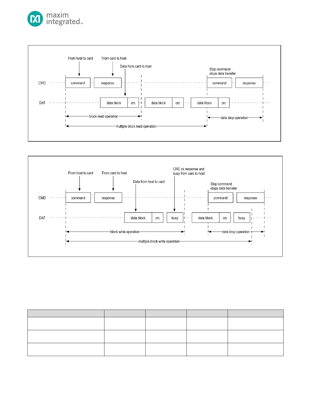
Figure 8-9: SD Bus Protocol - Multi-Block Read Operation
Figure 8-10: SD Bus Protocol - Multi Block Write Operation
8.5.4 SD Command Generation
Table 8-44 shows the registers required for three transaction types: SDMA generated transactions, ADMA generated
transactions, and CPU transactions (includes data transfers and Non-DAT transfers). When initiating a transaction, you
should program the registers sequentially starting with the SDHC_SDMA register and finishing with the SDHC_CMD register.
When the upper byte of the SDHC_CMD register is written, it triggers the SDHC to issue the SD command.
Table 8-44: Registers Used to Generate SD Commands
Register
SDMA Command
ADMA Command
CPU Data Transfer
Non-DAT (No Data) Transfer
SDMA System Address / Argument 2
SDHC_SDMA
Yes/No
No/Auto CMD23
No/AutoCMD23
No/No
Block Size
SDHC_BLK_SIZE
Yes
Yes
Yes
No (Protected)
Block Count
SDHC_BLK_CNT
Yes
Yes
Yes
No (Protected)

Table of Contents

Questions and Answers:

Question and Answer IconNeed help?

Do you have a question about the Maxim Integrated MAX32665 and is the answer not in the manual?

Maxim Integrated MAX32665 Specifications

General IconGeneral
BrandMaxim Integrated
ModelMAX32665
CategoryMotherboard
LanguageEnglish