16-40
Cisco ONS 15454 DWDM Installation and Operations Guide, R6.0
April 2006
Chapter 16 Card Reference
16.5.2 OPT-BST Amplifier Card
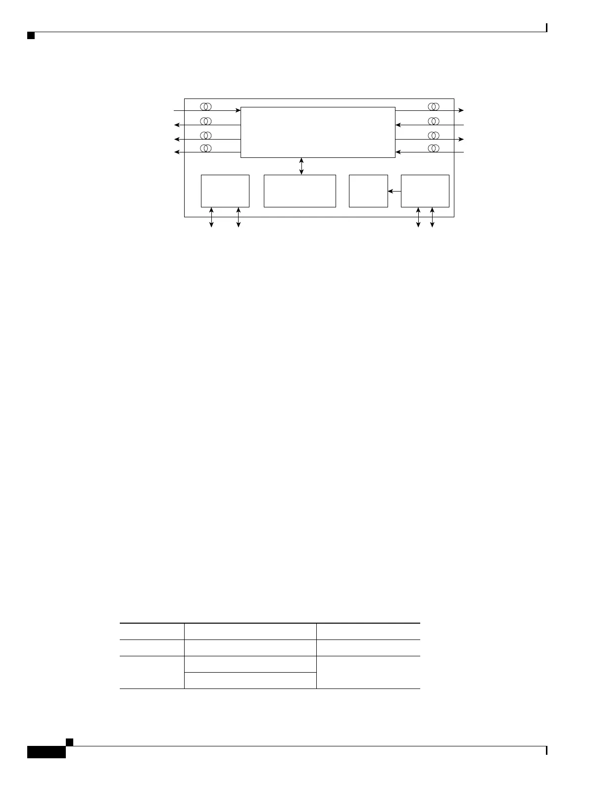
Figure 16-19 OPT-BST Block Diagram
Figure 16-20 shows the OPT-BST optical module functional block diagram.
Figure 16-20 OPT-BST Optical Module Functional Block Diagram
16.5.2.1 Power Monitoring
Physical photodiodes P1, P2, P3, and P4 monitor the power for the OPT-BST card. The returned power
level values are calibrated to the ports as shown in Table 16-22.
Optical
module
Line RX
Monitor Line RX
96479
Processor
Line TX
COM TX
Com RX
OSC TX
Monitor Line TX
OSC RX
FPGA
For SCL Bus
management
SCL Bus
TCCi M
SCL Bus
TCCi P
DC/DC
Power supply
Input filters
BAT A&B
Ta b l e 1 6 - 2 2 O P T- B S T Po r t C a l i b r a t i o n
Photodiode CTC Type Name Calibrated to Port
P1 Input Com COM RX
P2 Output Line (Total Output) LINE TX
Output Line (Signal Output)

 Loading...