(1) FTM reset
0x00160x00150x00140x00130x0011 . . .0x0010 0x00180x0017XXXX 0x0000 0x0012
FTM counter
CLKS[1:0]
channel (n) output
(4) write 1 to SC[CLKS]
(3) write any value
to CNT register
(2) FTM configuration
channel (n) pin is controlled by FTM
NOTES:
– CNTIN = 0x0010
– Channel (n) is in low-true combine mode with CNTIN < C(n)V < C(n+1)V < MOD
– C(n)V = 0x0015
00
XX
01
Figure 39-98. FTM behavior after reset when the channel (n) is in Combine mode
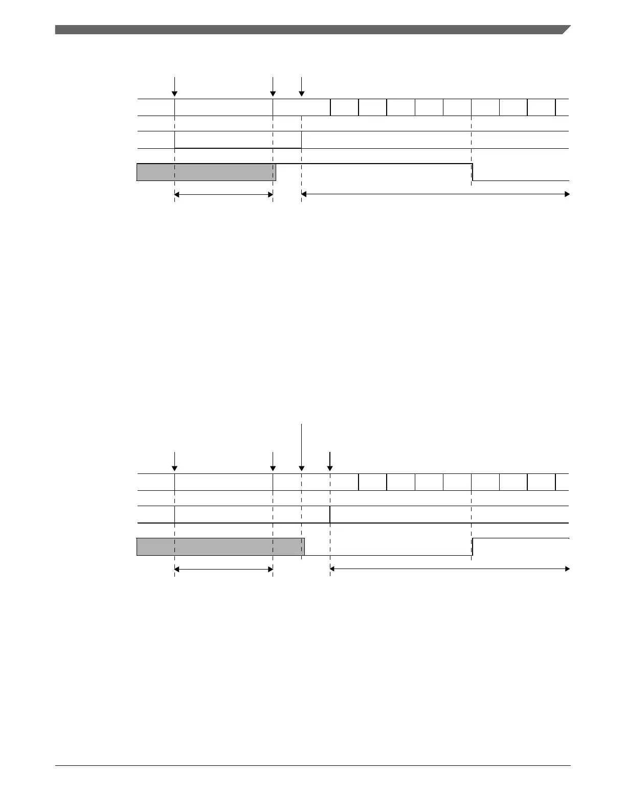
The following figure shows an example when the channel (n) is in Output Compare mode
and the channel (n) output is toggled when there is a match. In the Output Compare
mode, the channel output is not updated to its initial value when there is a write to CNT
register (item 3). In this case, use the software output control (Software output control) or
the initialization (Initialization) to update the channel output to the selected value (item
4).
(1) FTM reset
0x00150x00140x00130x0012 . . .0x0010 0x00170x0016XXXX 0x0000 0x0011
FTM counter
CLKS[1:0]
channel (n) output
(5) write 1 to SC[CLKS]
(3) write any value
to CNT register
(2) FTM configuration
channel (n) pin is controlled by FTM
NOTES:
– CNTIN = 0x0010
– Channel (n) is in output compare and the channel (n) output is toggled when there is a match
– C(n)V = 0x0014
00
XX
01
(4) use of software output control or initialization
to update the channel output to the zero
Figure 39-99. FTM behavior after reset when the channel (n) is in Output Compare mode
39.6
FTM Interrupts
Chapter 39 FlexTimer Module (FTM)
K22F Sub-Family Reference Manual, Rev. 4, 08/2016
NXP Semiconductors 1025

 Loading...