MCG_C5 field descriptions (continued)
Field Description
5
PLLSTEN0
PLL Stop Enable
Enables the PLL Clock during Normal Stop. In Low Power Stop mode, the PLL clock gets disabled even if
PLLSTEN 0 =1. All other power modes, PLLSTEN 0 bit has no affect and does not enable the PLL Clock
to run if it is written to 1.
0 MCGPLLCLK is disabled in any of the Stop modes.
1
MCGPLLCLK is enabled if system is in Normal Stop mode.
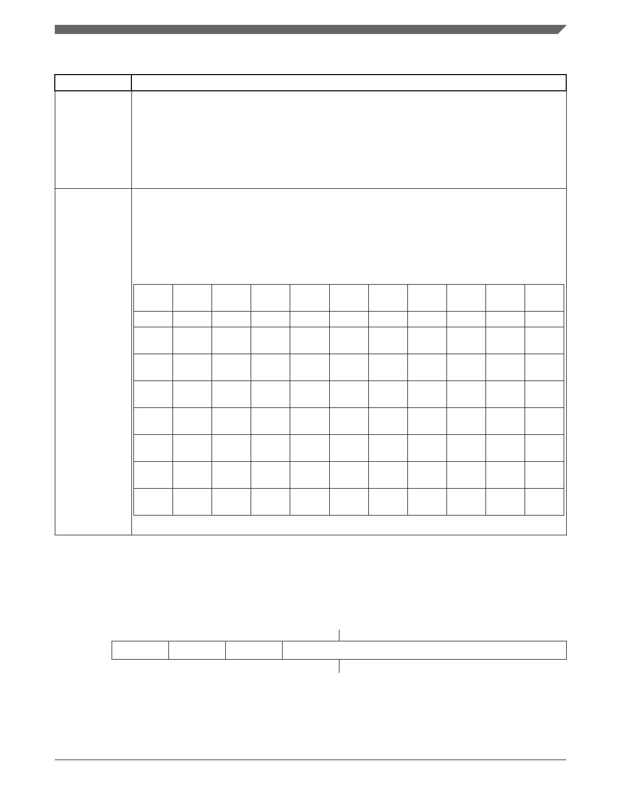
PRDIV0 PLL External Reference Divider
Selects the amount to divide down the external reference clock for the PLL. The resulting frequency must
be in the range of 2 MHz to 4 MHz. After the PLL is enabled (by setting either PLLCLKEN 0 or PLLS), the
PRDIV 0 value must not be changed when LOCK0 is zero.
Table 25-1. PLL External Reference Divide Factor
PRDIV
0
Divide
Factor
PRDIV
0
Divide
Factor
PRDIV
0
Divide
Factor
PRDIV
0
Divide
Factor
00000 1 01000 9 10000 17 11000 25
00001 2 01001 10 10001 18 11001 Reserve
d
00010 3 01010 11 10010 19 11010 Reserve
d
00011 4 01011 12 10011 20 11011 Reserve
d
00100 5 01100 13 10100 21 11100 Reserve
d
00101 6 01101 14 10101 22 11101 Reserve
d
00110 7 01110 15 10110 23 11110 Reserve
d
00111 8 01111 16 10111 24 11111 Reserve
d
25.3.6 MCG Control 6 Register (MCG_C6)
Address: 4006_4000h base + 5h offset = 4006_4005h
Bit 7 6 5 4 3 2 1 0
Read
LOLIE0 PLLS CME0 VDIV0
Write
Reset
0 0 0 0 0 0 0 0
Chapter 25 Multipurpose Clock Generator (MCG)
K22F Sub-Family Reference Manual, Rev. 4, 08/2016
NXP Semiconductors 549

 Loading...