51.4.3.2 Selecting an IEEE 1149.1-2001 register
Access to the JTAGC data registers is achieved by loading the instruction register with
any of the JTAGC block instructions while the JTAGC is enabled. Instructions are shifted
in via the Select-IR-Scan path and loaded in the Update-IR state. At this point, all data
register access is performed via the Select-DR-Scan path.
The Select-DR-Scan path is used to read or write the register data by shifting in the data
(LSB first) during the Shift-DR state. When reading a register, the register value is loaded
into the IEEE 1149.1-2001 shifter during the Capture-DR state. When writing a register,
the value is loaded from the IEEE 1149.1-2001 shifter to the register during the Update-
DR state. When reading a register, there is no requirement to shift out the entire register
contents. Shifting may be terminated once the required number of bits have been
acquired.
51.4.4
JTAGC block instructions
The JTAGC block implements the IEEE 1149.1-2001 defined instructions listed in the
following table. This section gives an overview of each instruction; refer to the IEEE
1149.1-2001 standard for more details. All undefined opcodes are reserved.
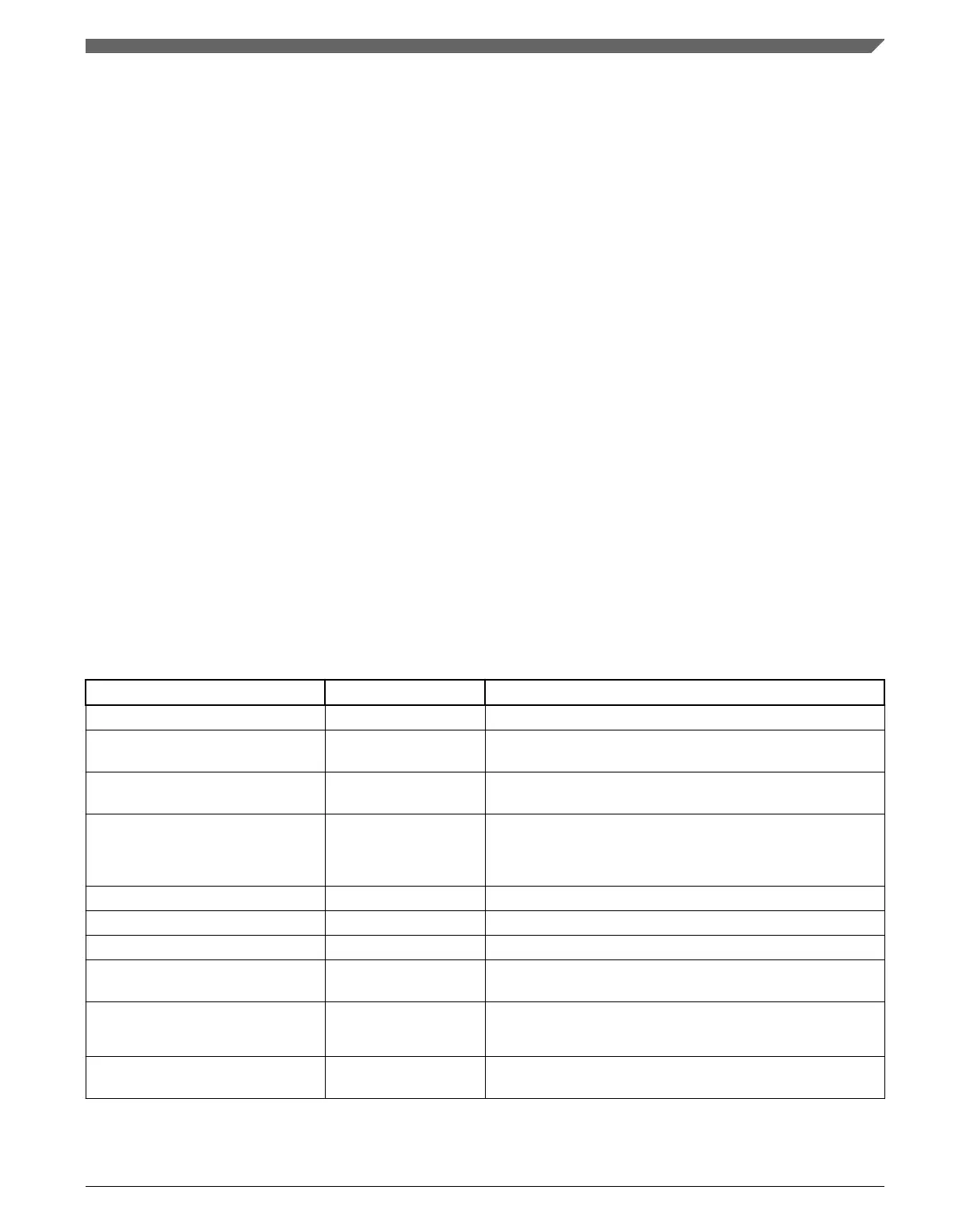
Table 51-3. 4-bit JTAG instructions
Instruction Code[3:0] Instruction summary
IDCODE 0000 Selects device identification register for shift
SAMPLE/PRELOAD 0010 Selects boundary scan register for shifting, sampling, and
preloading without disturbing functional operation
SAMPLE 0011 Selects boundary scan register for shifting and sampling
without disturbing functional operation
EXTEST 0100 Selects boundary scan register and applies preloaded values
to output pins.
NOTE:
Execution of this instruction asserts functional reset.
Factory debug reserved 0101 Intended for factory debug only
Factory debug reserved 0110 Intended for factory debug only
Factory debug reserved 0111 Intended for factory debug only
ARM JTAG-DP Reserved 1000 This instruction goes the ARM JTAG-DP controller. See the
ARM JTAG-DP documentation for more information.
HIGHZ 1001 Selects bypass register and three-states all output pins.
NOTE:
Execution of this instruction asserts functional reset.
ARM JTAG-DP Reserved 1010 This instruction goes the ARM JTAG-DP controller. See the
ARM JTAG-DP documentation for more information.
Table continues on the next page...
Chapter 51 JTAG Controller (JTAGC)
K22F Sub-Family Reference Manual, Rev. 4, 08/2016
NXP Semiconductors 1391

 Loading...