31.1.2 Features
FlexBus offers the following features:
• Six independent, user-programmable chip-select signals (FB_CS5 –FB_CS0)
• 8-bit, 16-bit, and 32-bit transfers
• Programmable burst and burst-inhibited transfers selectable for each chip-select and
transfer direction
• Programmable address-setup time with respect to the assertion of a chip-select
• Programmable address-hold time with respect to the deassertion of a chip-select and
transfer direction
• Extended address latch enable option to assist with glueless connections to
synchronous and asynchronous memory devices
31.2
Signal descriptions
This table describes the external signals involved in data-transfer operations.
NOTE
Not all of the following signals may be available on a particular
device. See the Chip Configuration details for information on
which signals are available.
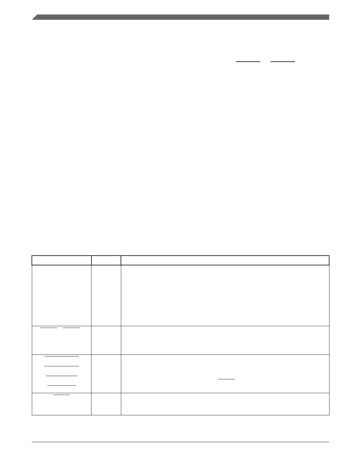
Table 31-1. FlexBus signal descriptions
Signal I/O Function
FB_AD31 - FB_AD0 I/O This is the address and data bus, FB_AD.
The number of byte lanes carrying the data is determined by the port size associated
with the matching chip-select.
The full 32-bit address is driven on the first clock of a bus cycle (address phase). After
the first clock, the data is driven on the bus (data phase). During the data phase, the
address is driven on the pins not used for data. For example, in 16-bit mode, the lower
address is driven on FB_AD15–FB_AD0, and in 8-bit mode, the lower address is driven
on FB_AD23–FB_AD0.
FB_CS5–FB_CS0 O General Purpose Chip-Selects—Indicate which external memory or peripheral is
selected. A particular chip-select is asserted when the transfer address is within the
external memory's or peripheral's address space, as defined in CSAR[BA] and
CSMR[BAM].
FB_BE_31_24
FB_BE_23_16
FB_BE_15_8
FB_BE_7_0
O Byte Enables—Indicate that data is to be latched or driven onto a specific byte lane of
the data bus. CSCR[BEM] determines if these signals are asserted on reads and writes
or on writes only.
For external SRAM or flash devices, the FB_BE outputs should be connected to
individual byte strobe signals.
FB_OE O Output Enable—Sent to the external memory or peripheral to enable a read transfer.
This signal is asserted during read accesses only when a chip-select matches the
current address decode.
Table continues on the next page...
Signal descriptions
K22F Sub-Family Reference Manual, Rev. 4, 08/2016
694 NXP Semiconductors

 Loading...