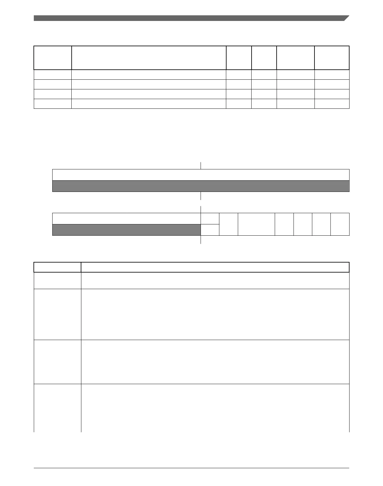
LPTMR memory map
Absolute
address
(hex)
Register name
Width
(in bits)
Access Reset value
Section/
page
4004_0000 Low Power Timer Control Status Register (LPTMR0_CSR) 32 R/W 0000_0000h 41.3.1/1043
4004_0004 Low Power Timer Prescale Register (LPTMR0_PSR) 32 R/W 0000_0000h 41.3.2/1044
4004_0008 Low Power Timer Compare Register (LPTMR0_CMR) 32 R/W 0000_0000h 41.3.3/1046
4004_000C Low Power Timer Counter Register (LPTMR0_CNR) 32 R/W 0000_0000h 41.3.4/1046
41.3.1 Low Power Timer Control Status Register (LPTMRx_CSR)
Address: 4004_0000h base + 0h offset = 4004_0000h
Bit 31 30 29 28 27 26 25 24 23 22 21 20 19 18 17 16
R
0
W
Reset
0 0 0 0 0 0 0 0 0 0 0 0 0 0 0 0
Bit
15 14 13 12 11 10 9 8 7 6 5 4 3 2 1 0
R
0 TCF
TIE TPS TPP TFC TMS TEN
W
w1c
Reset
0 0 0 0 0 0 0 0 0 0 0 0 0 0 0 0
LPTMRx_CSR field descriptions
Field Description
31–8
Reserved
This field is reserved.
This read-only field is reserved and always has the value 0.
7
TCF
Timer Compare Flag
TCF is set when the LPTMR is enabled and the CNR equals the CMR and increments. TCF is cleared
when the LPTMR is disabled or a logic 1 is written to it.
0 The value of CNR is not equal to CMR and increments.
1 The value of CNR is equal to CMR and increments.
6
TIE
Timer Interrupt Enable
When TIE is set, the LPTMR Interrupt is generated whenever TCF is also set.
0 Timer interrupt disabled.
1 Timer interrupt enabled.
5–4
TPS
Timer Pin Select
Configures the input source to be used in Pulse Counter mode. TPS must be altered only when the
LPTMR is disabled. The input connections vary by device. See the chip configuration details for
information on the connections to these inputs.
00 Pulse counter input 0 is selected.
Table continues on the next page...
Chapter 41 Low-Power Timer (LPTMR)
K22F Sub-Family Reference Manual, Rev. 4, 08/2016
NXP Semiconductors 1043

 Loading...