Program flash
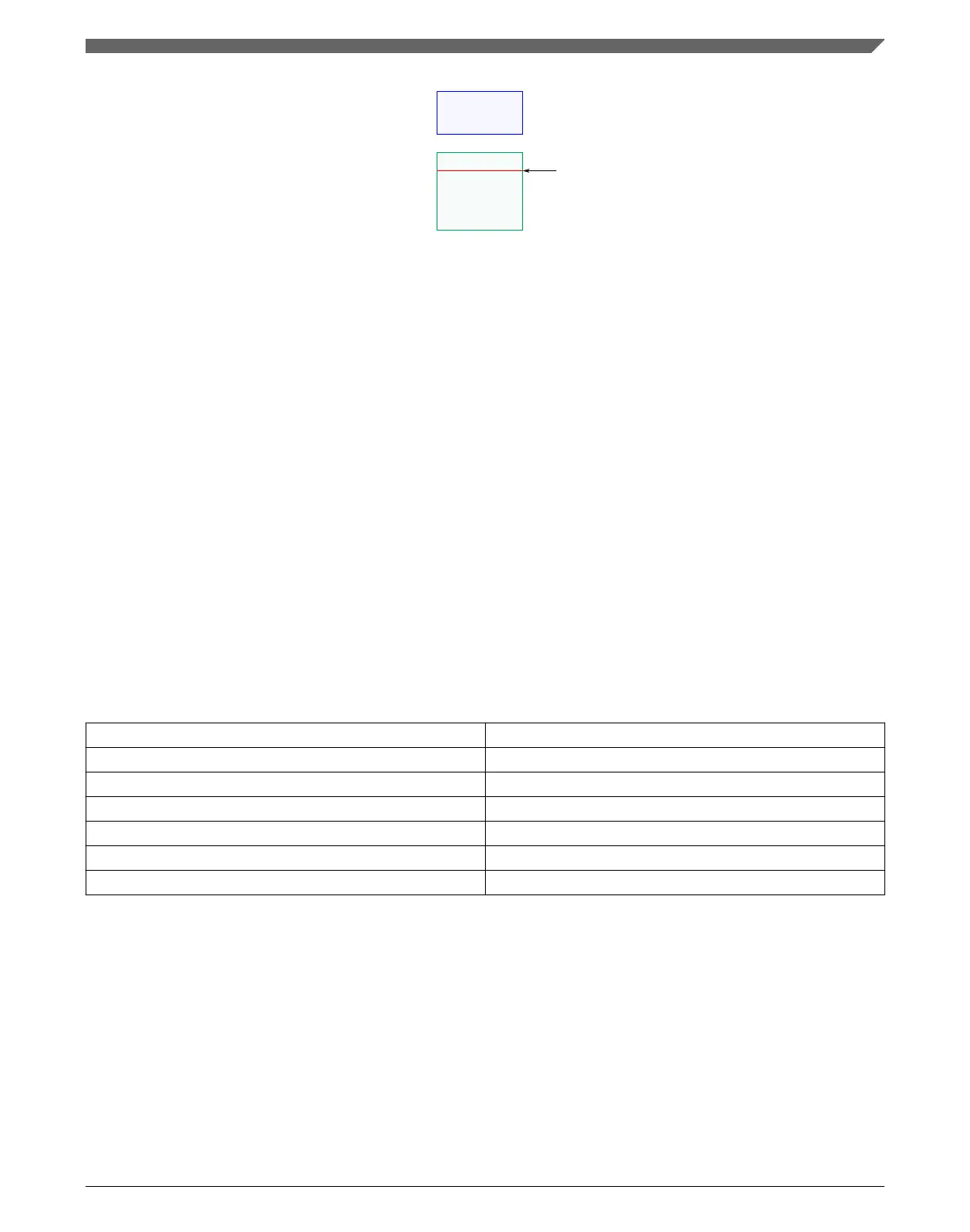
Flash configuration field
Program flash base address
Flash memory base address
Registers
Figure 4-2. Flash memory map
The on-chip Flash is implemented in a portion of the allocated Flash range to form a
contiguous block in the memory map beginning at address 0x0000_0000. See Flash
Memory Sizes for details of supported ranges.
Accesses to the flash memory ranges outside the amount of Flash on the device causes
the bus cycle to be terminated with an error followed by the appropriate response in the
requesting bus master. Read collision events in which flash memory is accessed while a
flash memory resource is being manipulated by a flash command also generates a bus
error response.
4.3.1
Alternate Non-Volatile IRC User Trim Description
The following non-volatile locations (4 bytes) are reserved for custom IRC user trim
supported by some development tools. An alternate IRC trim to the factory loaded trim
can be stored at this location. To override the factory trim, user software must load new
values into the MCG trim registers.
Non-Volatile Byte Address Alternate IRC Trim Value
0x0000_03FC Reserved
0x0000_03FD Reserved
0x0000_03FE (bit 0) SCFTRIM
0x0000_03FE (bit 4:1) FCTRIM
0x0000_03FE (bit 6) FCFTRIM
0x0000_03FF SCTRIM
4.4 SRAM memory map
The on-chip RAM is split in two regions: SRAM_L and SRAM_U. The RAM is
implemented such that the SRAM_L and SRAM_U ranges form a contiguous block in
the memory map. See SRAM Configuration for details.
Chapter 4 Memory Map
K22F Sub-Family Reference Manual, Rev. 4, 08/2016
NXP Semiconductors 143

 Loading...