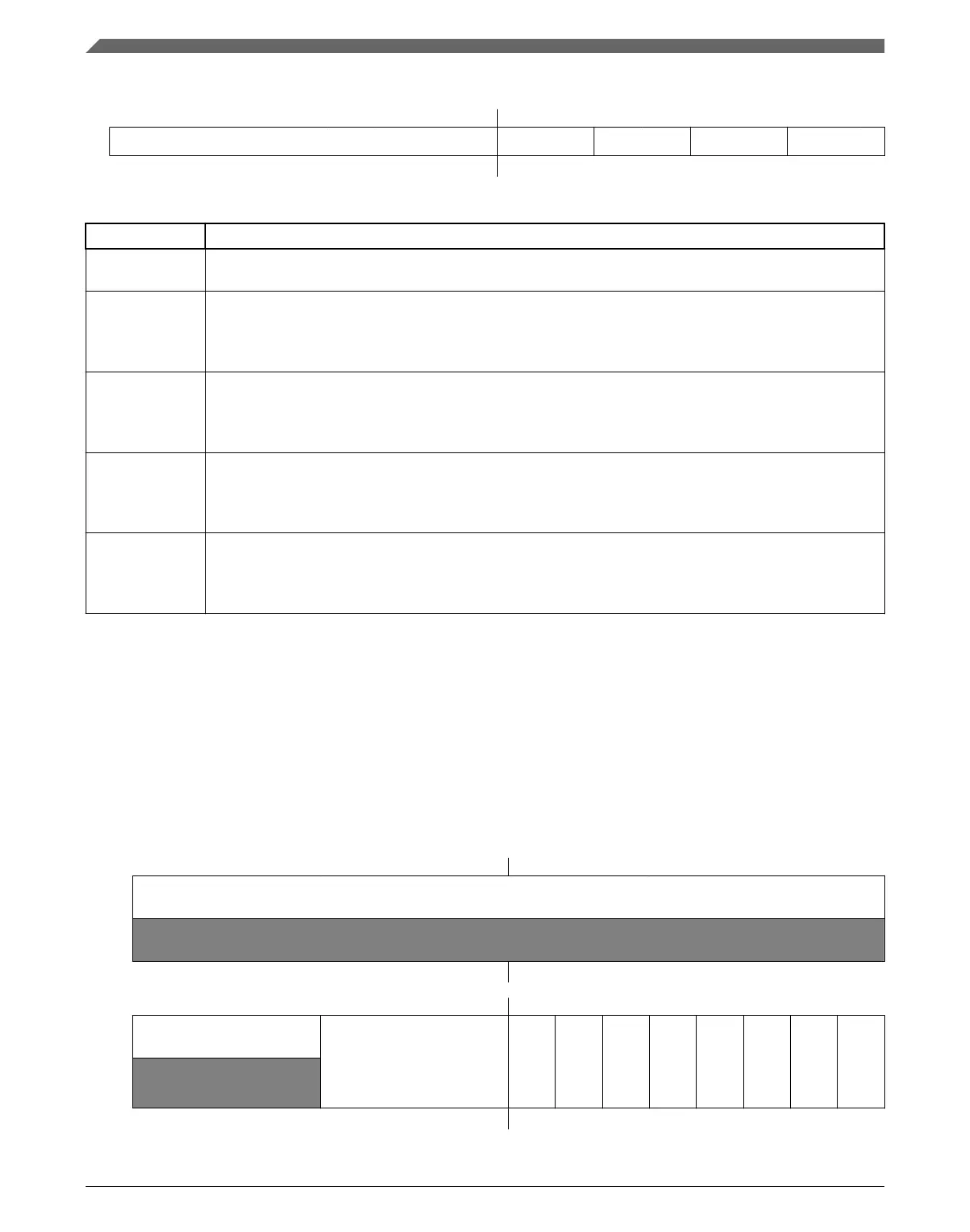
Address: Base address + 78h offset
Bit 31 30 29 28 27 26 25 24 23 22 21 20 19 18 17 16 15 14 13 12 11 10 9 8 7 6 5 4 3 2 1 0
R
Reserved CH3FVAL CH2FVAL CH1FVAL CH0FVAL
W
Reset
0 0 0 0 0 0 0 0 0 0 0 0 0 0 0 0 0 0 0 0 0 0 0 0 0 0 0 0 0 0 0 0
FTMx_FILTER field descriptions
Field Description
31–16
Reserved
This field is reserved.
15–12
CH3FVAL
Channel 3 Input Filter
Selects the filter value for the channel input.
The filter is disabled when the value is zero.
11–8
CH2FVAL
Channel 2 Input Filter
Selects the filter value for the channel input.
The filter is disabled when the value is zero.
7–4
CH1FVAL
Channel 1 Input Filter
Selects the filter value for the channel input.
The filter is disabled when the value is zero.
CH0FVAL Channel 0 Input Filter
Selects the filter value for the channel input.
The filter is disabled when the value is zero.
39.3.20 Fault Control (FTMx_FLTCTRL)
This register selects the filter value for the fault inputs, enables the fault inputs and the
fault inputs filter.
Address:
Base address + 7Ch offset
Bit 31 30 29 28 27 26 25 24 23 22 21 20 19 18 17 16
R
0
W
Reset
0 0 0 0 0 0 0 0 0 0 0 0 0 0 0 0
Bit
15 14 13 12 11 10 9 8 7 6 5 4 3 2 1 0
R
0
FFVAL
FFLTR3EN
FFLTR2EN
FFLTR1EN
FFLTR0EN
FAULT3EN
FAULT2EN
FAULT1EN
FAULT0EN
W
Reset
0 0 0 0 0 0 0 0 0 0 0 0 0 0 0 0
Memory map and register definition
K22F Sub-Family Reference Manual, Rev. 4, 08/2016
932 NXP Semiconductors

 Loading...