2. Set the control level to 2 via zero-bit scans
3. Execute the Store Format (STFMT) command (00011) to set the scan format register
to 1149.7 scan format
9.3 Debug Port Pin Descriptions
The debug port pins default after POR to their JTAG functionality with the exception of
JTAG_TRST_b and can be later reassigned to their alternate functionalities. In cJTAG
and SWD modes JTAG_TDI and JTAG_TRST_b can be configured to alternate GPIO
functions.
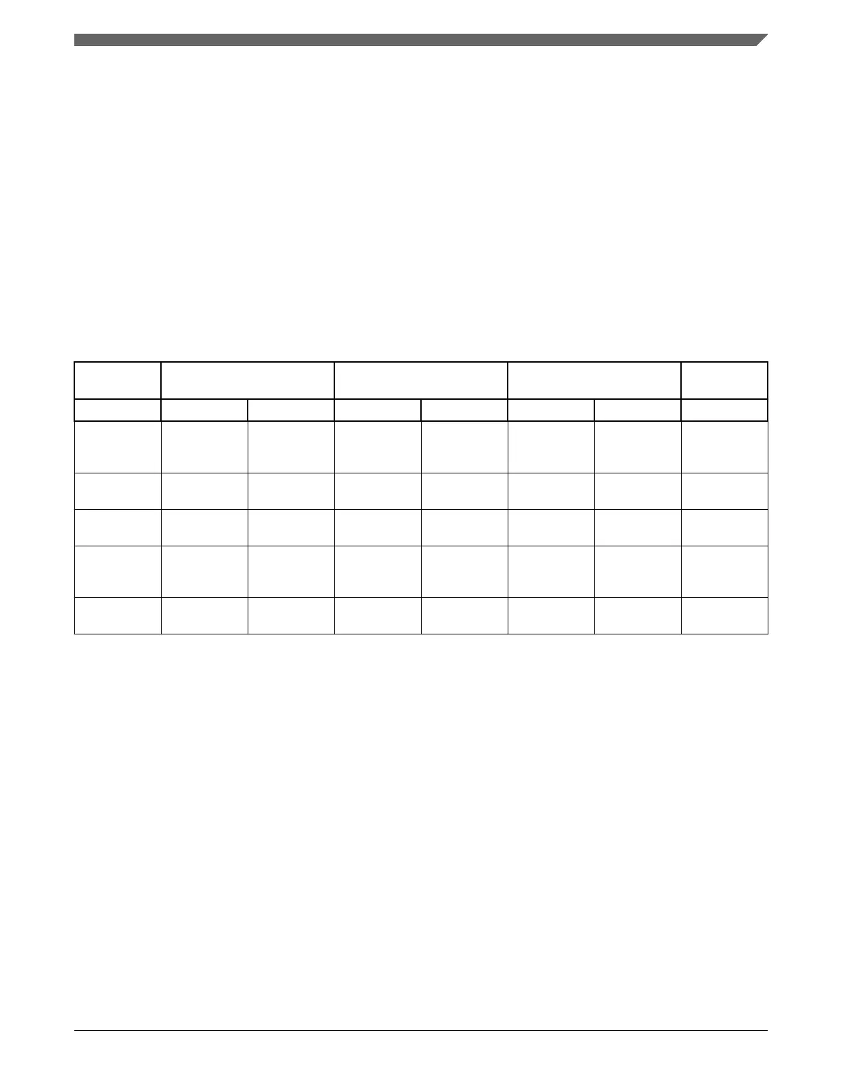
Table 9-2. Debug port pins
Pin Name JTAG Debug Port cJTAG Debug Port SWD Debug Port Internal Pull-
up\Down
Type Description Type Description Type Description
JTAG_TMS/
SWD_DIO
I JTAG Test
Mode
Selection
I cJTAG Data I/O Serial Wire
Data
Pull-up
JTAG_TCLK/
SWD_CLK
I JTAG Test
Clock
I cJTAG Clock I Serial Wire
Clock
Pull-down
JTAG_TDI I JTAG Test
Data Input
- - - - Pull-up
JTAG_TDO/
TRACE_SWO
O JTAG Test
Data Output
O Trace output
over a single
pin
O Trace output
over a single
pin
N/C
JTAG_TRST_
b
I JTAG Reset I cJTAG Reset - - Pull-up
9.4 System TAP connection
The system JTAG controller is connected in parallel to the ARM TAP controller. The
system JTAG controller IR codes overlay the ARM JTAG controller IR codes without
conflict. Refer to the IR codes table for a list of the available IR codes. The output of the
TAPs (TDO) are muxed based on the IR code which is selected. This design is fully
JTAG compliant and appears to the JTAG chain as a single TAP. At power on reset,
ARM's IDCODE (IR=4'b1110) is selected.
Chapter 9 Debug
K22F Sub-Family Reference Manual, Rev. 4, 08/2016
NXP Semiconductors 203

 Loading...