36.4.1 DAC Data Low Register (DACx_DATnL)
Address: Base address + 0h offset + (2d × i), where i=0d to 15d
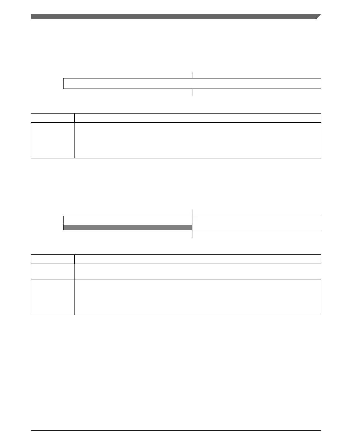
Bit 7 6 5 4 3 2 1 0
Read
DATA0
Write
Reset
0 0 0 0 0 0 0 0
DACx_DATnL field descriptions
Field Description
DATA0 DATA0
When the DAC buffer is not enabled, DATA[11:0] controls the output voltage based on the following
formula: V
out
= V
in
* (1 + DACDAT0[11:0])/4096
When the DAC buffer is enabled, DATA is mapped to the 16-word buffer.
36.4.2 DAC Data High Register (DACx_DATnH)
Address: Base address + 1h offset + (2d × i), where i=0d to 15d
Bit 7 6 5 4 3 2 1 0
Read 0
DATA1
Write
Reset
0 0 0 0 0 0 0 0
DACx_DATnH field descriptions
Field Description
7–4
Reserved
This field is reserved.
This read-only field is reserved and always has the value 0.
DATA1 DATA1
When the DAC Buffer is not enabled, DATA[11:0] controls the output voltage based on the following
formula. V
out
= V
in
* (1 + DACDAT0[11:0])/4096
When the DAC buffer is enabled, DATA[11:0] is mapped to the 16-word buffer.
Chapter 36 12-bit Digital-to-Analog Converter (DAC)
K22F Sub-Family Reference Manual, Rev. 4, 08/2016
NXP Semiconductors 849

 Loading...