MCG_C3 field descriptions (continued)
Field Description
An additional fine trim bit is available in C4 register as the SCFTRIM bit. Upon reset, this value is loaded
with a factory trim value.
If an SCTRIM value stored in nonvolatile memory is to be used, it is your responsibility to copy that value
from the nonvolatile memory location to this register.
1. A value for SCTRIM is loaded during reset from a factory programmed location.
25.3.4 MCG Control 4 Register (MCG_C4)
Address: 4006_4000h base + 3h offset = 4006_4003h
Bit 7 6 5 4 3 2 1 0
Read
DMX32 DRST_DRS FCTRIM SCFTRIM
Write
Reset
0 0 0 x* x* x* x* x*
* Notes:
x = Undefined at reset.•
MCG_C4 field descriptions
Field Description
7
DMX32
DCO Maximum Frequency with 32.768 kHz Reference
The DMX32 bit controls whether the DCO frequency range is narrowed to its maximum frequency with a
32.768 kHz reference.
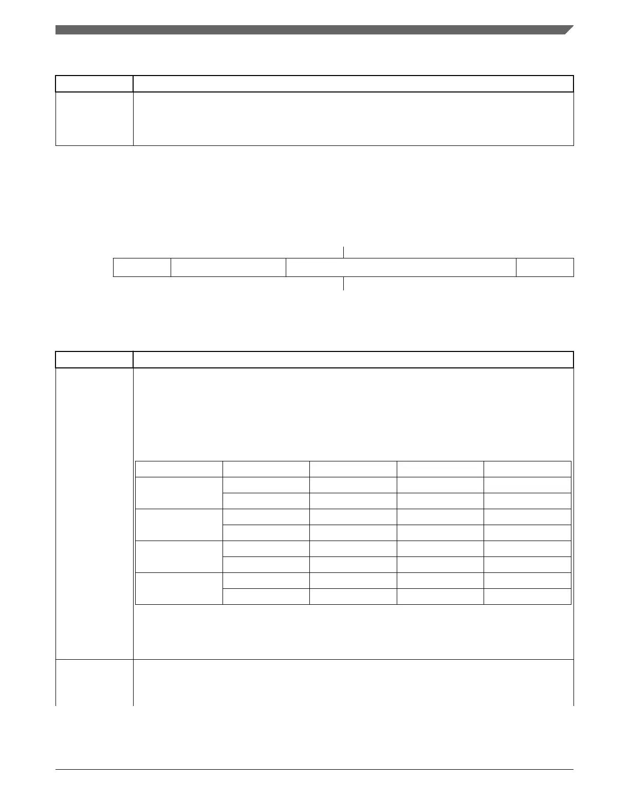
The following table identifies settings for the DCO frequency range.
NOTE:
The system clocks derived from this source should not exceed their specified maximums.
DRST_DRS DMX32 Reference Range FLL Factor DCO Range
00 0 31.25–39.0625 kHz 640 20–25 MHz
1 32.768 kHz 732 24 MHz
01 0 31.25–39.0625 kHz 1280 40–50 MHz
1 32.768 kHz 1464 48 MHz
10 0 31.25–39.0625 kHz 1920 60–75 MHz
1 32.768 kHz 2197 72 MHz
11 0 31.25–39.0625 kHz 2560 80–100 MHz
1 32.768 kHz 2929 96 MHz
0 DCO has a default range of 25%.
1 DCO is fine-tuned for maximum frequency with 32.768 kHz reference.
6–5
DRST_DRS
DCO Range Select
The DRS bits select the frequency range for the FLL output, DCOOUT. When the LP bit is set, writes to
the DRS bits are ignored. The DRST read field indicates the current frequency range for DCOOUT. The
Table continues on the next page...
Chapter 25 Multipurpose Clock Generator (MCG)
K22F Sub-Family Reference Manual, Rev. 4, 08/2016
NXP Semiconductors 547

 Loading...