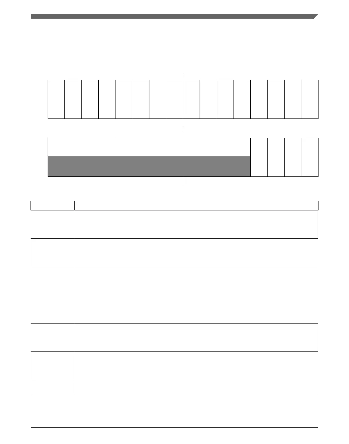
12.2.7 System Options Register 8 (SIM_SOPT8)
Address: 4004_7000h base + 101Ch offset = 4004_801Ch
Bit 31 30 29 28 27 26 25 24 23 22 21 20 19 18 17 16
R
FTM3OCH7SR
C
FTM3OCH6SR
C
FTM3OCH5SR
C
FTM3OCH4SR
C
FTM3OCH3SR
C
FTM3OCH2SR
C
FTM3OCH1SR
C
FTM3OCH0SR
C
FTM0OCH7SR
C
FTM0OCH6SR
C
FTM0OCH5SR
C
FTM0OCH4SR
C
FTM0OCH3SR
C
FTM0OCH2SR
C
FTM0OCH1SR
C
FTM0OCH0SR
C
W
Reset
0 0 0 0 0 0 0 0 0 0 0 0 0 0 0 0
Bit
15 14 13 12 11 10 9 8 7 6 5 4 3 2 1 0
R
0
FTM3SYNCBIT
FTM2SYNCBIT
FTM1SYNCBIT
FTM0SYNCBIT
W
Reset
0 0 0 0 0 0 0 0 0 0 0 0 0 0 0 0
SIM_SOPT8 field descriptions
Field Description
31
FTM3OCH7SRC
FTM3 channel 7 output source
0 FTM3_CH7 pin is output of FTM3 channel 7 output
1 FTM3_CH7 pin is output of FTM3 channel 7 output modulated by FTM2 channel 1 output.
30
FTM3OCH6SRC
FTM3 channel 6 output source
0 FTM3_CH6 pin is output of FTM3 channel 6 output
1 FTM3_CH6 pin is output of FTM3 channel 6 output modulated by FTM2 channel 1 output.
29
FTM3OCH5SRC
FTM3 channel 5 output source
0 FTM3_CH5 pin is output of FTM3 channel 5 output
1 FTM3_CH5 pin is output of FTM3 channel 5 output modulated by FTM2 channel 1 output.
28
FTM3OCH4SRC
FTM3 channel 4 output source
0 FTM3_CH4 pin is output of FTM3 channel 4 output
1 FTM3_CH4 pin is output of FTM3 channel 4 output modulated by FTM2 channel 1 output.
27
FTM3OCH3SRC
FTM3 channel 3 output source
0 FTM3_CH3 pin is output of FTM3 channel 3 output
1 FTM3_CH3 pin is output of FTM3 channel 3 output modulated by FTM2 channel 1 output.
26
FTM3OCH2SRC
FTM3 channel 2 output source
0 FTM3_CH2 pin is output of FTM3 channel 2 output
1 FTM3_CH2 pin is output of FTM3 channel 2 output modulated by FTM2 channel 1 output.
25
FTM3OCH1SRC
FTM3 channel 1 output source
Table continues on the next page...
Chapter 12 System Integration Module (SIM)
K22F Sub-Family Reference Manual, Rev. 4, 08/2016
NXP Semiconductors 273

 Loading...