25.1.2 Modes of Operation
The MCG has the following modes of operation: FEI, FEE, FBI, FBE, PBE, PEE, BLPI,
BLPE, and Stop. For details, see MCG modes of operation.
25.2 External Signal Description
There are no MCG signals that connect off chip.
25.3
Memory Map/Register Definition
This section includes the memory map and register definition.
The MCG registers can only be written when in supervisor mode. Write accesses when in
user mode will result in a bus error. Read accesses may be performed in both supervisor
and user mode.
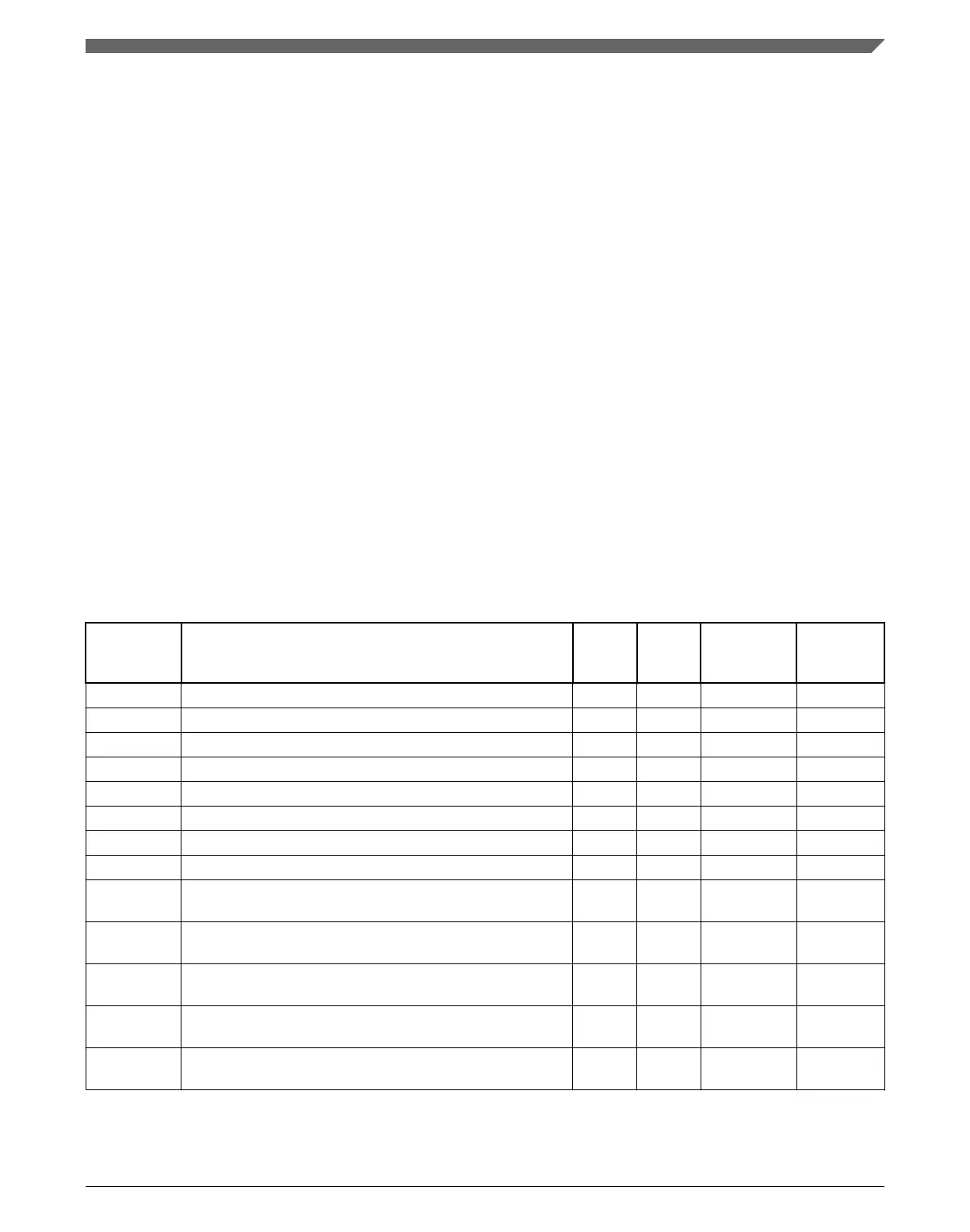
MCG memory map
Absolute
address
(hex)
Register name
Width
(in bits)
Access Reset value
Section/
page
4006_4000 MCG Control 1 Register (MCG_C1) 8 R/W 04h 25.3.1/544
4006_4001 MCG Control 2 Register (MCG_C2) 8 R/W See section 25.3.2/545
4006_4002 MCG Control 3 Register (MCG_C3) 8 R/W Undefined 25.3.3/546
4006_4003 MCG Control 4 Register (MCG_C4) 8 R/W See section 25.3.4/547
4006_4004 MCG Control 5 Register (MCG_C5) 8 R/W 00h 25.3.5/548
4006_4005 MCG Control 6 Register (MCG_C6) 8 R/W 00h 25.3.6/549
4006_4006 MCG Status Register (MCG_S) 8 R 10h 25.3.7/551
4006_4008 MCG Status and Control Register (MCG_SC) 8 R/W 02h 25.3.8/552
4006_400A
MCG Auto Trim Compare Value High Register
(MCG_ATCVH)
8 R/W 00h 25.3.9/554
4006_400B
MCG Auto Trim Compare Value Low Register
(MCG_ATCVL)
8 R/W 00h
25.3.10/
554
4006_400C MCG Control 7 Register (MCG_C7) 8 R/W 00h
25.3.11/
554
4006_400D MCG Control 8 Register (MCG_C8) 8 R/W 80h
25.3.12/
555
4006_4011 MCG Control 12 Register (MCG_C12) 8 R/W 00h
25.3.13/
556
Table continues on the next page...
Chapter 25 Multipurpose Clock Generator (MCG)
K22F Sub-Family Reference Manual, Rev. 4, 08/2016
NXP Semiconductors 543

 Loading...