42.2 Register definition
All registers must be accessed using 32-bit writes and all register accesses incur three
wait states.
Write accesses to any register by non-supervisor mode software, when the supervisor
access bit in the control register is clear, will terminate with a bus error.
Read accesses by non-supervisor mode software complete as normal.
Writing to a register protected by the write access register or lock register does not
generate a bus error, but the write will not complete.
Reading a register protected by the read access register does not generate a bus error, but
the register will read zero.
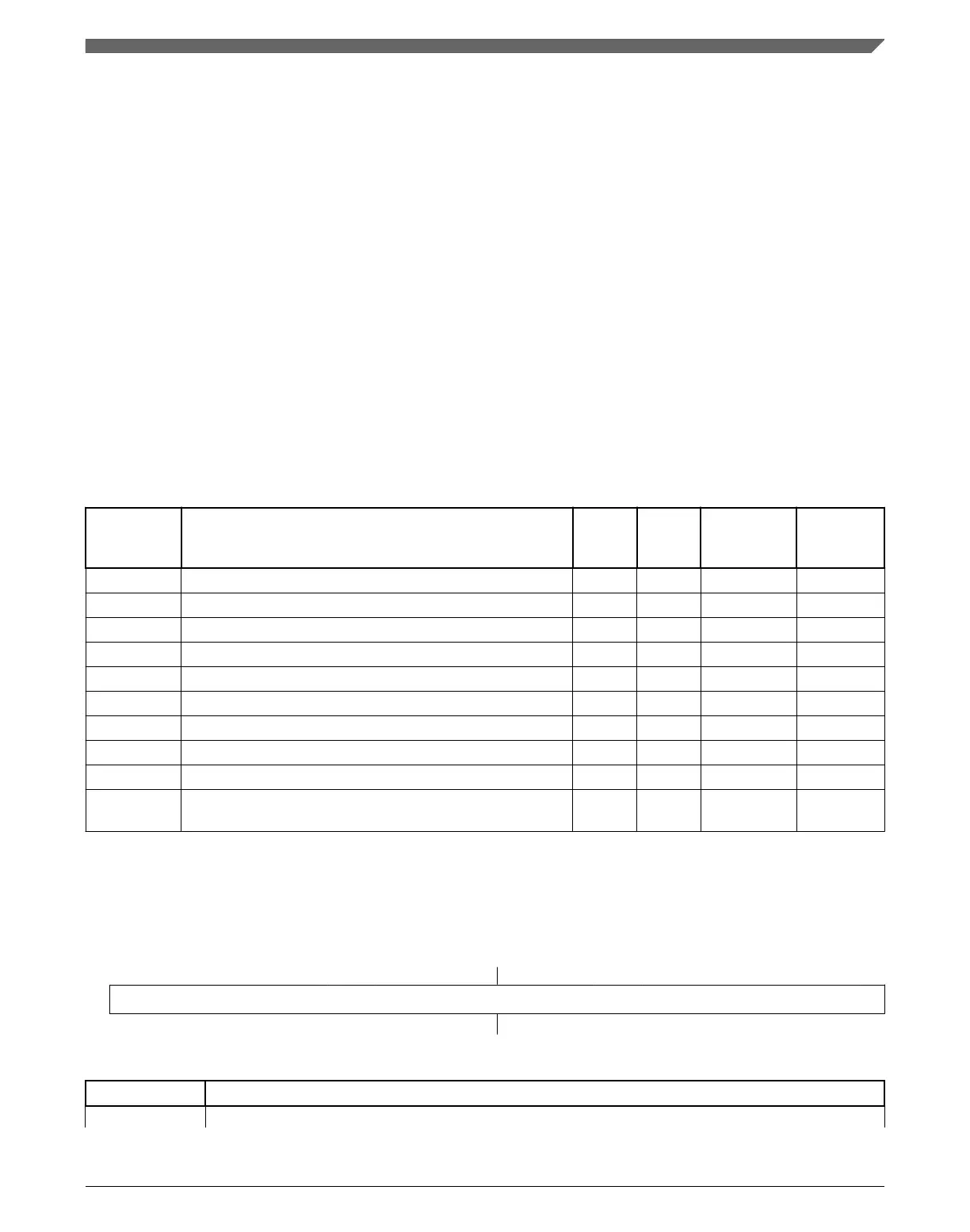
RTC memory map
Absolute
address
(hex)
Register name
Width
(in bits)
Access Reset value
Section/
page
4003_D000 RTC Time Seconds Register (RTC_TSR) 32 R/W 0000_0000h 42.2.1/1053
4003_D004 RTC Time Prescaler Register (RTC_TPR) 32 R/W 0000_0000h 42.2.2/1054
4003_D008 RTC Time Alarm Register (RTC_TAR) 32 R/W 0000_0000h 42.2.3/1054
4003_D00C RTC Time Compensation Register (RTC_TCR) 32 R/W 0000_0000h 42.2.4/1055
4003_D010 RTC Control Register (RTC_CR) 32 R/W 0000_0000h 42.2.5/1056
4003_D014 RTC Status Register (RTC_SR) 32 R/W 0000_0001h 42.2.6/1058
4003_D018 RTC Lock Register (RTC_LR) 32 R/W 0000_00FFh 42.2.7/1059
4003_D01C RTC Interrupt Enable Register (RTC_IER) 32 R/W 0000_0007h 42.2.8/1060
4003_D800 RTC Write Access Register (RTC_WAR) 32 R/W 0000_00FFh 42.2.9/1061
4003_D804 RTC Read Access Register (RTC_RAR) 32 R/W 0000_00FFh
42.2.10/
1062
42.2.1 RTC Time Seconds Register (RTC_TSR)
Address: 4003_D000h base + 0h offset = 4003_D000h
Bit 31 30 29 28 27 26 25 24 23 22 21 20 19 18 17 16 15 14 13 12 11 10 9 8 7 6 5 4 3 2 1 0
R
TSR
W
Reset
0 0 0 0 0 0 0 0 0 0 0 0 0 0 0 0 0 0 0 0 0 0 0 0 0 0 0 0 0 0 0 0
RTC_TSR field descriptions
Field Description
TSR Time Seconds Register
Chapter 42 Real Time Clock (RTC)
K22F Sub-Family Reference Manual, Rev. 4, 08/2016
NXP Semiconductors 1053

 Loading...