SC1A
ADHWTSA
ADHWTSn
C o m p a re tru e
A D C H
c o m p le te
A D T R G
A D C O
Control Registers
SC1n
A D IV
A D IC L K
Async
Clock Gen
A D A C K E N
ALTCLK
ADACK
A D C K
M O D E
tra n s fe r
C V 2
CV1:CV2
TempM
DADM3
DADM0
DADP3
DADP0
Interrupt
1
A D V IN P
A D V IN M
A C F E
1
SC2
Rn
RA
CFG1,2
C L M x
CLMx
Compare true
MCU STOP
ADHWT
AD4
AD23
TempP
V
REFH
V
ALTH
V
REFL
V
ALTL
AIEN
C O C O
trig g e r
DIFF
M O D E
CLPx
PG, MG
PG, MG
CLPx
Calibration
OFS
CALF
CAL
SC3
C V1
ACFGT, ACREN
D
AVGE, AVGS
ADCOFS
V
REFSH
V
REFSL
(SC2, CFG1, CFG2)
Conversion
trigger
control
Clock
divide
Control sequencer
Bus clock
SAR converter
Compare
logic
Offset subtractor
Averager
Formatting
ADLSMP/ADLSTS
ADLPC/ADHSC
initialize
sample
convert
transfer
abort
ALTCLK2
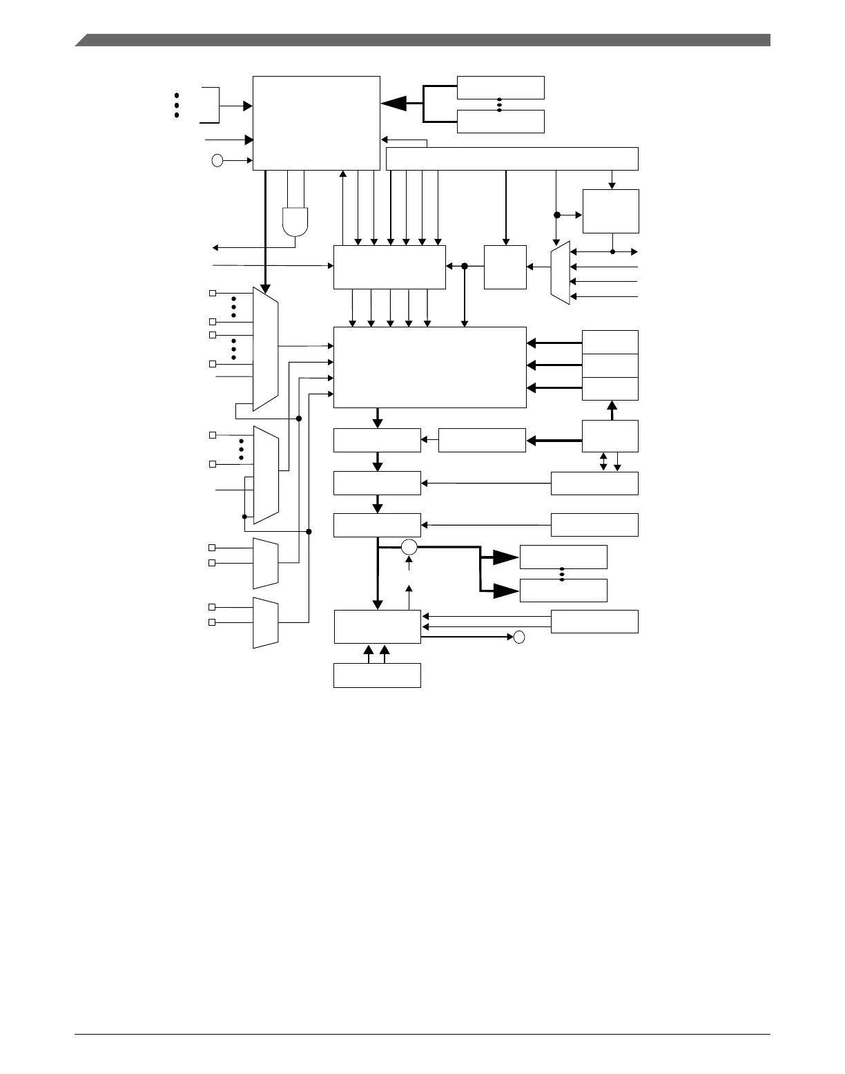
Figure 34-1. ADC block diagram
34.2
ADC signal descriptions
The ADC module supports up to 4 pairs of differential inputs and up to 24 single-ended
inputs.
Each differential pair requires two inputs, DADPx and DADMx. The ADC also requires
four supply/reference/ground connections.
ADC signal descriptions
K22F Sub-Family Reference Manual, Rev. 4, 08/2016
764 NXP Semiconductors

 Loading...