6 BITS
TRM
SC[VREFEN]
2 BITS
SC[MODE_LV]
REGULATION
BUFFER
BANDGAP
100 nF
VREF_OUT
OUTPUT PIN
SC[VREFST]
1.75 V Regulator
1.75 V
VDDA
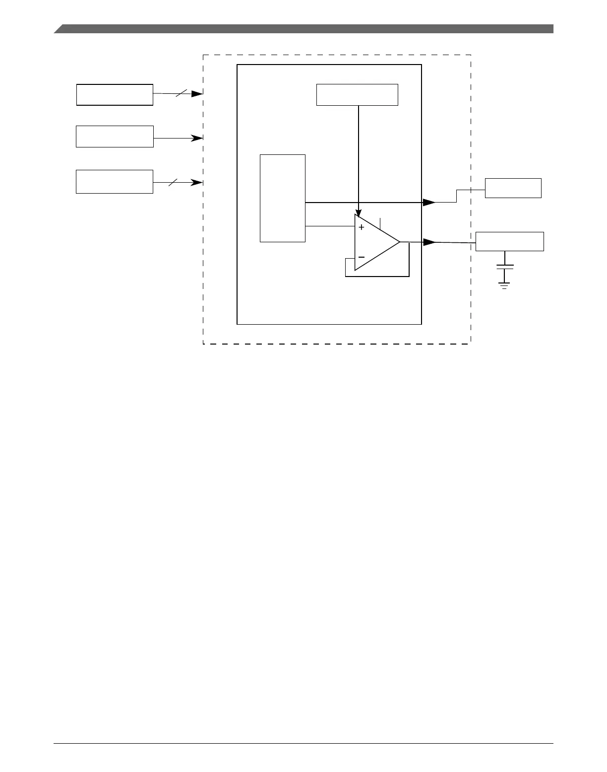
Figure 37-1. Voltage reference block diagram
37.1.1
Overview
The Voltage Reference provides a buffered reference voltage for use as an external
reference. In addition, the buffered reference is available internally for use with on chip
peripherals such as ADCs and DACs. Refer to the chip configuration details for a
description of these options. The reference voltage signal is output on a dedicated output
pin when the VREF is enabled. The Voltage Reference output can be trimmed with a
resolution of 0.5mV by means of the TRM register TRIM[5:0] bitfield.
37.1.2
Features
The Voltage Reference has the following features:
• Programmable trim register with 0.5 mV steps, automatically loaded with factory
trimmed value upon reset
• Programmable buffer mode selection:
• Off
Introduction
K22F Sub-Family Reference Manual, Rev. 4, 08/2016
858 NXP Semiconductors

 Loading...