Name Function I/O
externally generated and an output generated
synchronously by the bit clock when internally
generated.
SAI_RX_DATA Receive Data. The receive data is sampled
synchronously by the bit clock.
I
SAI_MCLK Audio Master Clock. The master clock is an input
when externally generated and an output when
internally generated.
I/O
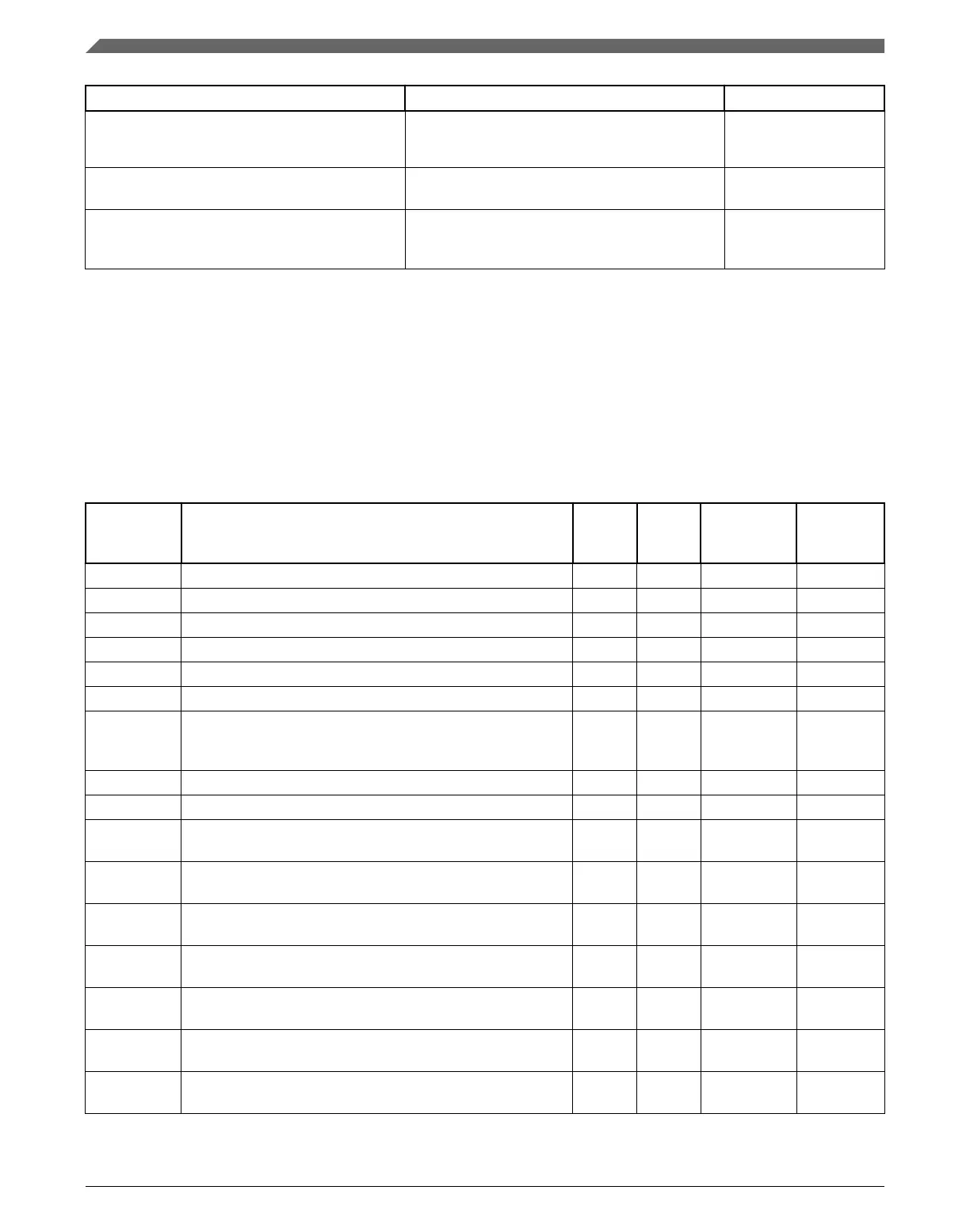
49.3 Memory map and register definition
A read or write access to an address from offset 0x108 and above will result in a bus
error.
I2S memory map
Absolute
address
(hex)
Register name
Width
(in bits)
Access Reset value
Section/
page
4002_F000 SAI Transmit Control Register (I2S0_TCSR) 32 R/W 0000_0000h 49.3.1/1341
4002_F004 SAI Transmit Configuration 1 Register (I2S0_TCR1) 32 R/W 0000_0000h 49.3.2/1344
4002_F008 SAI Transmit Configuration 2 Register (I2S0_TCR2) 32 R/W 0000_0000h 49.3.3/1345
4002_F00C SAI Transmit Configuration 3 Register (I2S0_TCR3) 32 R/W 0000_0000h 49.3.4/1346
4002_F010 SAI Transmit Configuration 4 Register (I2S0_TCR4) 32 R/W 0000_0000h 49.3.5/1347
4002_F014 SAI Transmit Configuration 5 Register (I2S0_TCR5) 32 R/W 0000_0000h 49.3.6/1349
4002_F020 SAI Transmit Data Register (I2S0_TDR0) 32
W
(always
reads 0)
0000_0000h 49.3.7/1350
4002_F040 SAI Transmit FIFO Register (I2S0_TFR0) 32 R 0000_0000h 49.3.8/1350
4002_F060 SAI Transmit Mask Register (I2S0_TMR) 32 R/W 0000_0000h 49.3.9/1351
4002_F080 SAI Receive Control Register (I2S0_RCSR) 32 R/W 0000_0000h
49.3.10/
1352
4002_F084 SAI Receive Configuration 1 Register (I2S0_RCR1) 32 R/W 0000_0000h
49.3.11/
1355
4002_F088 SAI Receive Configuration 2 Register (I2S0_RCR2) 32 R/W 0000_0000h
49.3.12/
1355
4002_F08C SAI Receive Configuration 3 Register (I2S0_RCR3) 32 R/W 0000_0000h
49.3.13/
1357
4002_F090 SAI Receive Configuration 4 Register (I2S0_RCR4) 32 R/W 0000_0000h
49.3.14/
1358
4002_F094 SAI Receive Configuration 5 Register (I2S0_RCR5) 32 R/W 0000_0000h
49.3.15/
1360
4002_F0A0 SAI Receive Data Register (I2S0_RDR0) 32 R 0000_0000h
49.3.16/
1360
Table continues on the next page...
Memory map and register definition
K22F Sub-Family Reference Manual, Rev. 4, 08/2016
1340 NXP Semiconductors

 Loading...