12.2.11 System Clock Gating Control Register 6 (SIM_SCGC6)
Address: 4004_7000h base + 103Ch offset = 4004_803Ch
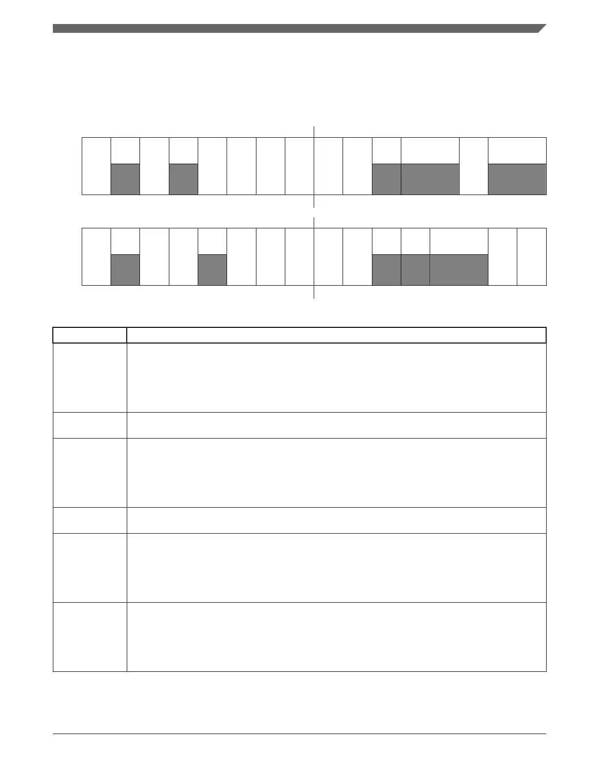
Bit 31 30 29 28 27 26 25 24 23 22 21 20 19 18 17 16
R
DAC0
1
RTC
0
ADC0
FTM2
FTM1
FTM0
PIT PDB
0 0
CRC
0
W
Reset
0 1 0 0 0 0 0 0 0 0 0 0 0 0 0 0
Bit
15 14 13 12 11 10 9 8 7 6 5 4 3 2 1 0
R
I2S
0
SPI1 SPI0
0
LPUART0
RNGA
DAC1
ADC1
FTM3
0 0 0
DMAMUX
FTF
W
Reset
0 0 0 0 0 0 0 0 0 0 0 0 0 0 0 1
SIM_SCGC6 field descriptions
Field Description
31
DAC0
DAC0 Clock Gate Control
This bit controls the clock gate to the DAC0 module.
0 Clock disabled
1 Clock enabled
30
Reserved
This field is reserved.
This read-only field is reserved and always has the value 1.
29
RTC
RTC Access Control
This bit controls software access and interrupts to the RTC module.
0 Access and interrupts disabled
1 Access and interrupts enabled
28
Reserved
This field is reserved.
This read-only field is reserved and always has the value 0.
27
ADC0
ADC0 Clock Gate Control
This bit controls the clock gate to the ADC0 module.
0 Clock disabled
1 Clock enabled
26
FTM2
FTM2 Clock Gate Control
This bit controls the clock gate to the FTM2 module.
0 Clock disabled
1 Clock enabled
Table continues on the next page...
Chapter 12 System Integration Module (SIM)
K22F Sub-Family Reference Manual, Rev. 4, 08/2016
NXP Semiconductors 281

 Loading...
