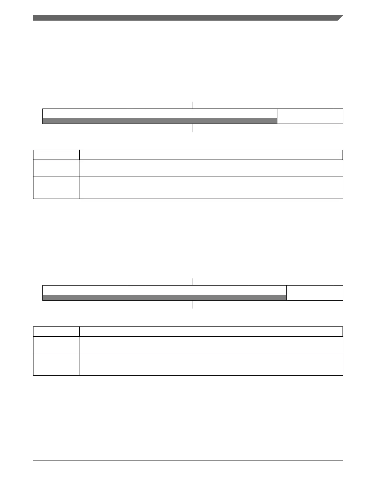
34.3.16 ADC Plus-Side General Calibration Value Register
(ADCx_CLP1)
For more information, see CLPD register description.
Address: Base address + 48h offset
Bit 31 30 29 28 27 26 25 24 23 22 21 20 19 18 17 16 15 14 13 12 11 10 9 8 7 6 5 4 3 2 1 0
R
0
CLP1
W
Reset
0 0 0 0 0 0 0 0 0 0 0 0 0 0 0 0 0 0 0 0 0 0 0 0 0 1 0 0 0 0 0 0
ADCx_CLP1 field descriptions
Field Description
31–7
Reserved
This field is reserved.
This read-only field is reserved and always has the value 0.
CLP1 Calibration Value
Calibration Value
34.3.17 ADC Plus-Side General Calibration Value Register
(ADCx_CLP0)
For more information, see CLPD register description.
Address:
Base address + 4Ch offset
Bit 31 30 29 28 27 26 25 24 23 22 21 20 19 18 17 16 15 14 13 12 11 10 9 8 7 6 5 4 3 2 1 0
R
0
CLP0
W
Reset
0 0 0 0 0 0 0 0 0 0 0 0 0 0 0 0 0 0 0 0 0 0 0 0 0 0 1 0 0 0 0 0
ADCx_CLP0 field descriptions
Field Description
31–6
Reserved
This field is reserved.
This read-only field is reserved and always has the value 0.
CLP0 Calibration Value
Calibration Value
Chapter 34 Analog-to-Digital Converter (ADC)
K22F Sub-Family Reference Manual, Rev. 4, 08/2016
NXP Semiconductors 785

 Loading...
