NOTE
For the number of channels supported on this device as well as
information regarding other chip-specific inputs into the ADC
block, see the chip-specific ADC configuration information.
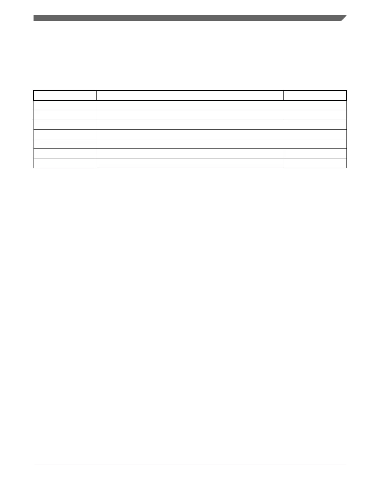
Table 34-1. ADC signal descriptions
Signal Description I/O
DADP3–DADP0 Differential Analog Channel Inputs I
DADM3–DADM0 Differential Analog Channel Inputs I
ADn Single-Ended Analog Channel Inputs I
V
REFSH
Voltage Reference Select High I
V
REFSL
Voltage Reference Select Low I
V
DDA
Analog Power Supply I
V
SSA
Analog Ground I
34.2.1 Analog Power (V
DDA
)
The ADC analog portion uses V
DDA
as its power connection. In some packages, V
DDA
is
connected internally to V
DD
. If externally available, connect the V
DDA
pin to the same
voltage potential as V
DD
. External filtering may be necessary to ensure clean V
DDA
for
good results.
34.2.2
Analog Ground (V
SSA
)
The ADC analog portion uses V
SSA
as its ground connection. In some packages, V
SSA
is
connected internally to V
SS
. If externally available, connect the V
SSA
pin to the same
voltage potential as V
SS
.
34.2.3
Voltage Reference Select
V
REFSH
and V
REFSL
are the high and low reference voltages for the ADC module.
The ADC can be configured to accept one of two voltage reference pairs for V
REFSH
and
V
REFSL
. Each pair contains a positive reference that must be between the minimum Ref
Voltage High and V
DDA
, and a ground reference that must be at the same potential as
V
SSA
. The two pairs are external (V
REFH
and V
REFL
) and alternate (V
ALTH
and V
ALTL
).
These voltage references are selected using SC2[REFSEL]. The alternate V
ALTH
and
Chapter 34 Analog-to-Digital Converter (ADC)
K22F Sub-Family Reference Manual, Rev. 4, 08/2016
NXP Semiconductors 765

 Loading...
