I2Cx_F field descriptions (continued)
Field Description
The SDA hold time is the delay from the falling edge of SCL (I2C clock) to the changing of SDA (I2C data).
SDA hold time = I2C module clock period (s) × mul × SDA hold value
The SCL start hold time is the delay from the falling edge of SDA (I2C data) while SCL is high (start
condition) to the falling edge of SCL (I2C clock).
SCL start hold time = I2C module clock period (s) × mul × SCL start hold value
The SCL stop hold time is the delay from the rising edge of SCL (I2C clock) to the rising edge of SDA (I2C
data) while SCL is high (stop condition).
SCL stop hold time = I2C module clock period (s) × mul × SCL stop hold value
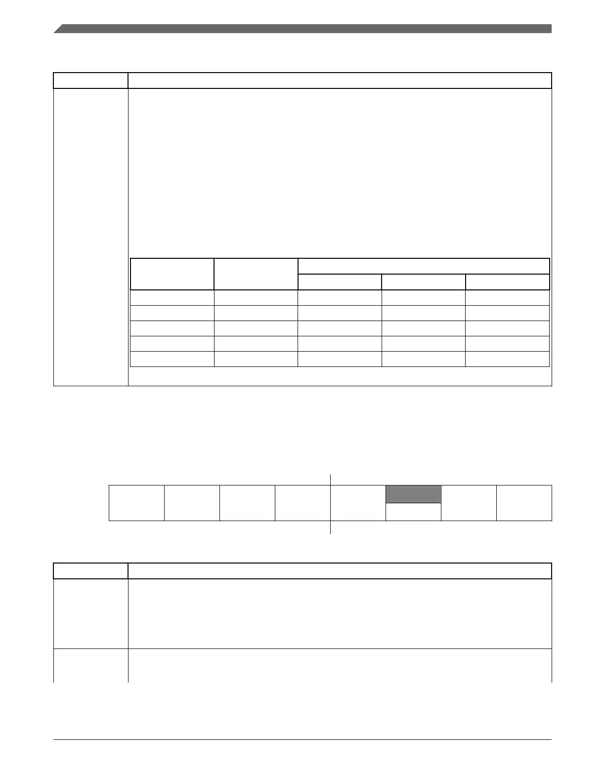
For example, if the I2C module clock speed is 8 MHz, the following table shows the possible hold time
values with different ICR and MULT selections to achieve an I
2
C baud rate of 100 kbit/s.
MULT ICR
Hold times (μs)
SDA SCL Start SCL Stop
2h 00h 3.500 3.000 5.500
1h 07h 2.500 4.000 5.250
1h 0Bh 2.250 4.000 5.250
0h 14h 2.125 4.250 5.125
0h 18h 1.125 4.750 5.125
46.3.3 I2C Control Register 1 (I2Cx_C1)
Address: Base address + 2h offset
Bit 7 6 5 4 3 2 1 0
Read
IICEN IICIE MST TX TXAK
0
WUEN DMAEN
Write RSTA
Reset
0 0 0 0 0 0 0 0
I2Cx_C1 field descriptions
Field Description
7
IICEN
I2C Enable
Enables I2C module operation.
0 Disabled
1 Enabled
6
IICIE
I2C Interrupt Enable
Enables I2C interrupt requests.
Table continues on the next page...
Memory map/register definition
K22F Sub-Family Reference Manual, Rev. 4, 08/2016
1186 NXP Semiconductors

 Loading...