PDBx_CHnC1 field descriptions (continued)
Field Description
These bits enable the PDB ADC pre-trigger operation as back-to-back mode. Only lower M pre-trigger bits
are implemented in this MCU. Back-to-back operation enables the ADC conversions complete to trigger
the next PDB channel pre-trigger and trigger output, so that the ADC conversions can be triggered on next
set of configuration and results registers. Application code must only enable the back-to-back operation of
the PDB pre-triggers at the leading of the back-to-back connection chain.
0 PDB channel's corresponding pre-trigger back-to-back operation disabled.
1 PDB channel's corresponding pre-trigger back-to-back operation enabled.
15–8
TOS
PDB Channel Pre-Trigger Output Select
Selects the PDB ADC pre-trigger outputs. Only lower M pre-trigger fields are implemented in this MCU.
0 PDB channel's corresponding pre-trigger is in bypassed mode. The pre-trigger asserts one peripheral
clock cycle after a rising edge is detected on selected trigger input source or software trigger is
selected and SWTRIG is written with 1.
1 PDB channel's corresponding pre-trigger asserts when the counter reaches the channel delay register
and one peripheral clock cycle after a rising edge is detected on selected trigger input source or
software trigger is selected and SETRIG is written with 1.
EN PDB Channel Pre-Trigger Enable
These bits enable the PDB ADC pre-trigger outputs. Only lower M pre-trigger bits are implemented in this
MCU.
0 PDB channel's corresponding pre-trigger disabled.
1 PDB channel's corresponding pre-trigger enabled.
38.3.6 Channel n Status register (PDBx_CHnS)
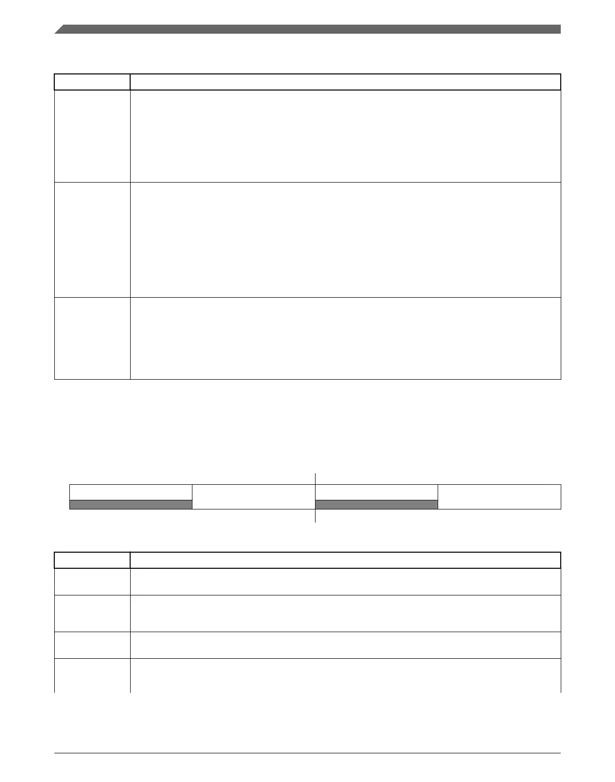
Address: 4003_6000h base + 14h offset + (40d × i), where i=0d to 1d
Bit 31 30 29 28 27 26 25 24 23 22 21 20 19 18 17 16 15 14 13 12 11 10 9 8 7 6 5 4 3 2 1 0
R
0
CF
0
ERR
W
Reset
0 0 0 0 0 0 0 0 0 0 0 0 0 0 0 0 0 0 0 0 0 0 0 0 0 0 0 0 0 0 0 0
PDBx_CHnS field descriptions
Field Description
31–24
Reserved
This field is reserved.
This read-only field is reserved and always has the value 0.
23–16
CF
PDB Channel Flags
The CF[m] bit is set when the PDB counter matches the CHnDLYm. Write 0 to clear these bits.
15–8
Reserved
This field is reserved.
This read-only field is reserved and always has the value 0.
ERR PDB Channel Sequence Error Flags
Only the lower M bits are implemented in this MCU.
Table continues on the next page...
Memory map and register definition
K22F Sub-Family Reference Manual, Rev. 4, 08/2016
878 NXP Semiconductors

 Loading...