1. When RCSR[RE] is first set
2. At the end of each frame
This allows the masked words in each frame to change from frame to frame.
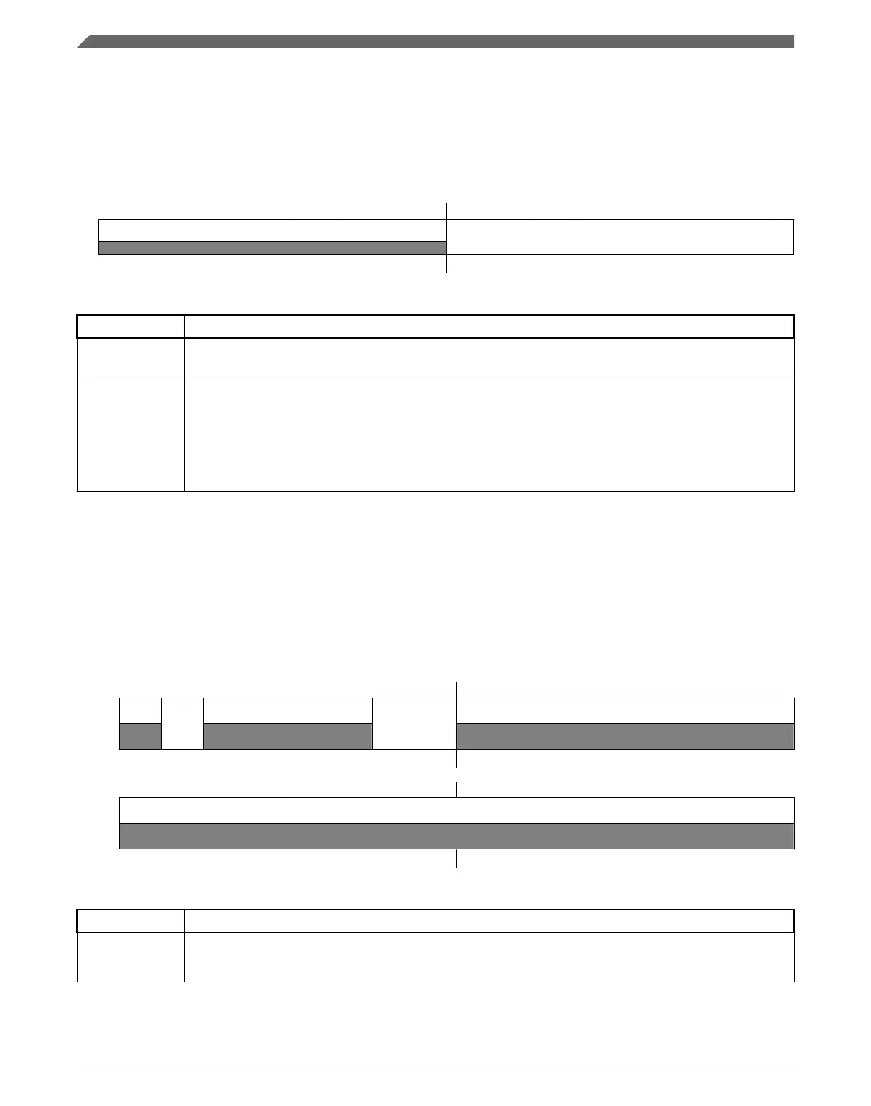
Address: 4002_F000h base + E0h offset = 4002_F0E0h
Bit 31 30 29 28 27 26 25 24 23 22 21 20 19 18 17 16 15 14 13 12 11 10 9 8 7 6 5 4 3 2 1 0
R
0
RWM
W
Reset
0 0 0 0 0 0 0 0 0 0 0 0 0 0 0 0 0 0 0 0 0 0 0 0 0 0 0 0 0 0 0 0
I2Sx_RMR field descriptions
Field Description
31–16
Reserved
This field is reserved.
This read-only field is reserved and always has the value 0.
RWM Receive Word Mask
Configures whether the receive word is masked (received data ignored and not written to receive FIFO) for
the corresponding word in the frame.
0 Word N is enabled.
1 Word N is masked.
49.3.19 SAI MCLK Control Register (I2Sx_MCR)
The MCLK Control Register (MCR) controls the clock source and direction of the audio
master clock.
Address:
4002_F000h base + 100h offset = 4002_F100h
Bit 31 30 29 28 27 26 25 24 23 22 21 20 19 18 17 16
R
DUF
MOE
0
MICS
0
W
Reset
0 0 0 0 0 0 0 0 0 0 0 0 0 0 0 0
Bit
15 14 13 12 11 10 9 8 7 6 5 4 3 2 1 0
R
0
W
Reset
0 0 0 0 0 0 0 0 0 0 0 0 0 0 0 0
I2Sx_MCR field descriptions
Field Description
31
DUF
Divider Update Flag
Provides the status of on-the-fly updates to the MCLK divider ratio.
Table continues on the next page...
Memory map and register definition
K22F Sub-Family Reference Manual, Rev. 4, 08/2016
1362 NXP Semiconductors

 Loading...