10.4.7 Communication Interfaces
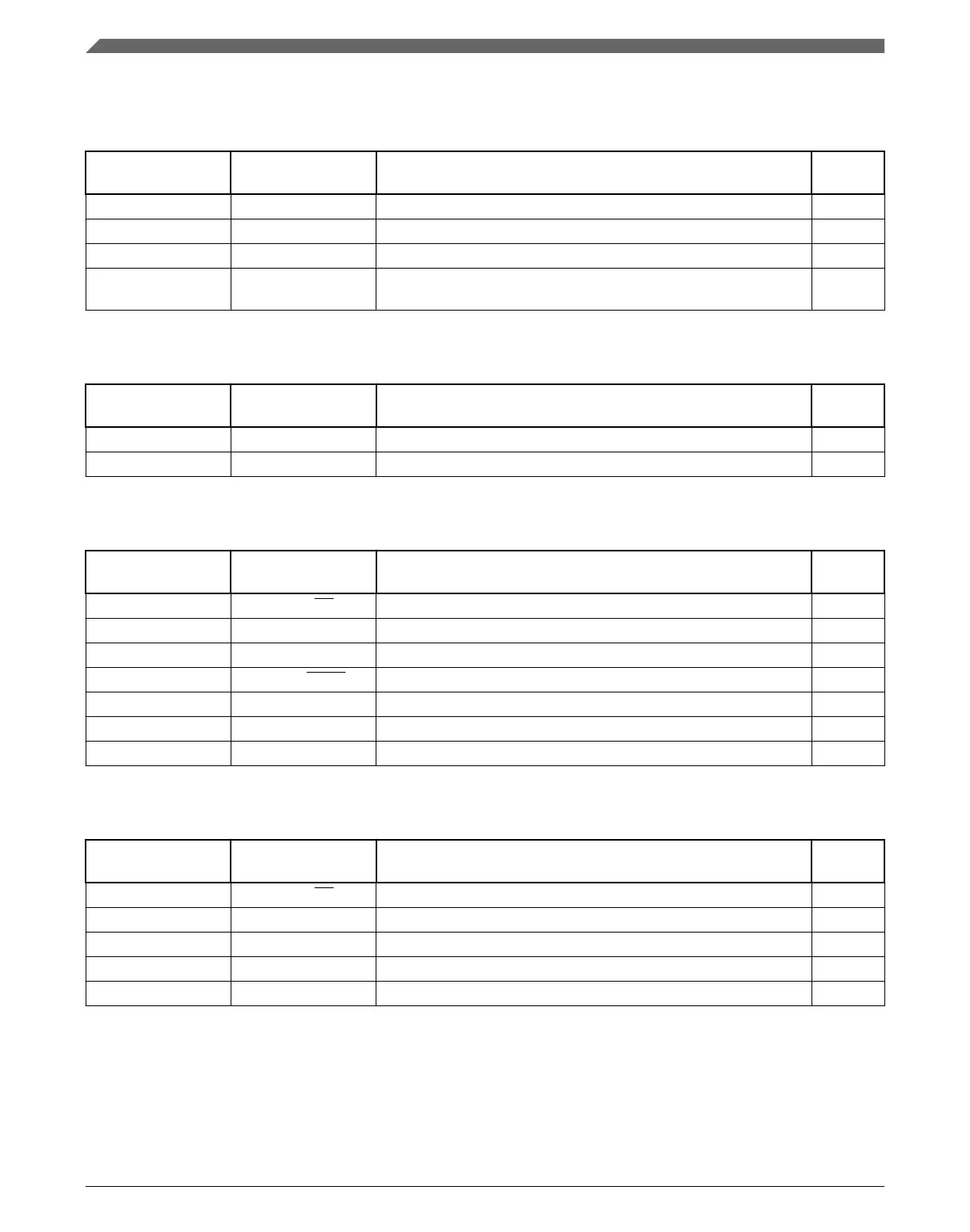
Table 10-25. USB FS OTG Signal Descriptions
Chip signal name Module signal
name
Description I/O
USB0_DM usb_dm USB D- analog data signal on the USB bus. I/O
USB0_DP usb_dp USB D+ analog data signal on the USB bus. I/O
USB_CLKIN — Alternate USB clock input I
USB_SOF_OUT — USB start of frame signal. Can be used to make the USB start of
frame available for external synchronization.
O
Table 10-26. USB VREG Signal Descriptions
Chip signal name Module signal
name
Description I/O
VOUT33 reg33_out Regulator output voltage O
VREGIN reg33_in Unregulated power supply I
Table 10-27. SPI 0 Signal Descriptions
Chip signal name Module signal
name
Description I/O
SPI0_PCS0 PCS0/SS Peripheral Chip Select 0 (O) I/O
SPI0_PCS[3:1] PCS[1:3] Peripheral Chip Selects 1–3 O
SPI0_PCS4 PCS4 Peripheral Chip Select 4 O
SPI0_PCS5 PCS5/ PCSS Peripheral Chip Select 5 /Peripheral Chip Select Strobe O
SPI0_SIN SIN Serial Data In I
SPI0_SOUT SOUT Serial Data Out O
SPI0_SCK SCK Serial Clock (O) I/O
Table 10-28. SPI 1 Signal Descriptions
Chip signal name Module signal
name
Description I/O
SPI1_PCS0 PCS0/SS Peripheral Chip Select 0 (O) I/O
SPI1_PCS[3:1] PCS[1:3] Peripheral Chip Selects 1–3 O
SPI1_SIN SIN Serial Data In I
SPI1_SOUT SOUT Serial Data Out O
SPI1_SCK SCK Serial Clock (O) I/O
Module Signal Description Tables
K22F Sub-Family Reference Manual, Rev. 4, 08/2016
236 NXP Semiconductors

 Loading...