V
ALTL
voltage reference pair may select additional external pins or internal sources
depending on MCU configuration. See the chip configuration information on the Voltage
References specific to this MCU.
In some packages, V
REFH
is connected in the package to V
DDA
and V
REFL
to V
SSA
. If
externally available, the positive reference(s) may be connected to the same potential as
V
DDA
or may be driven by an external source to a level between the minimum Ref
Voltage High and the V
DDA
potential. V
REFH
must never exceed V
DDA
. Connect the
ground references to the same voltage potential as V
SSA
.
34.2.4 Analog Channel Inputs (ADx)
The ADC module supports up to 24 single-ended analog inputs. A single-ended input is
selected for conversion through the SC1[ADCH] channel select bits when SC1n[DIFF] is
low.
34.2.5
Differential Analog Channel Inputs (DADx)
The ADC module supports up to four differential analog channel inputs. Each differential
analog input is a pair of external pins, DADPx and DADMx, referenced to each other to
provide the most accurate analog to digital readings. A differential input is selected for
conversion through SC1[ADCH] when SC1n[DIFF] is high. All DADPx inputs may be
used as single-ended inputs if SC1n[DIFF] is low. In certain MCU configurations, some
DADMx inputs may also be used as single-ended inputs if SC1n[DIFF] is low. For ADC
connections specific to this device, see the chip-specific ADC information.
34.3
Memory map and register definitions
This section describes the ADC registers.
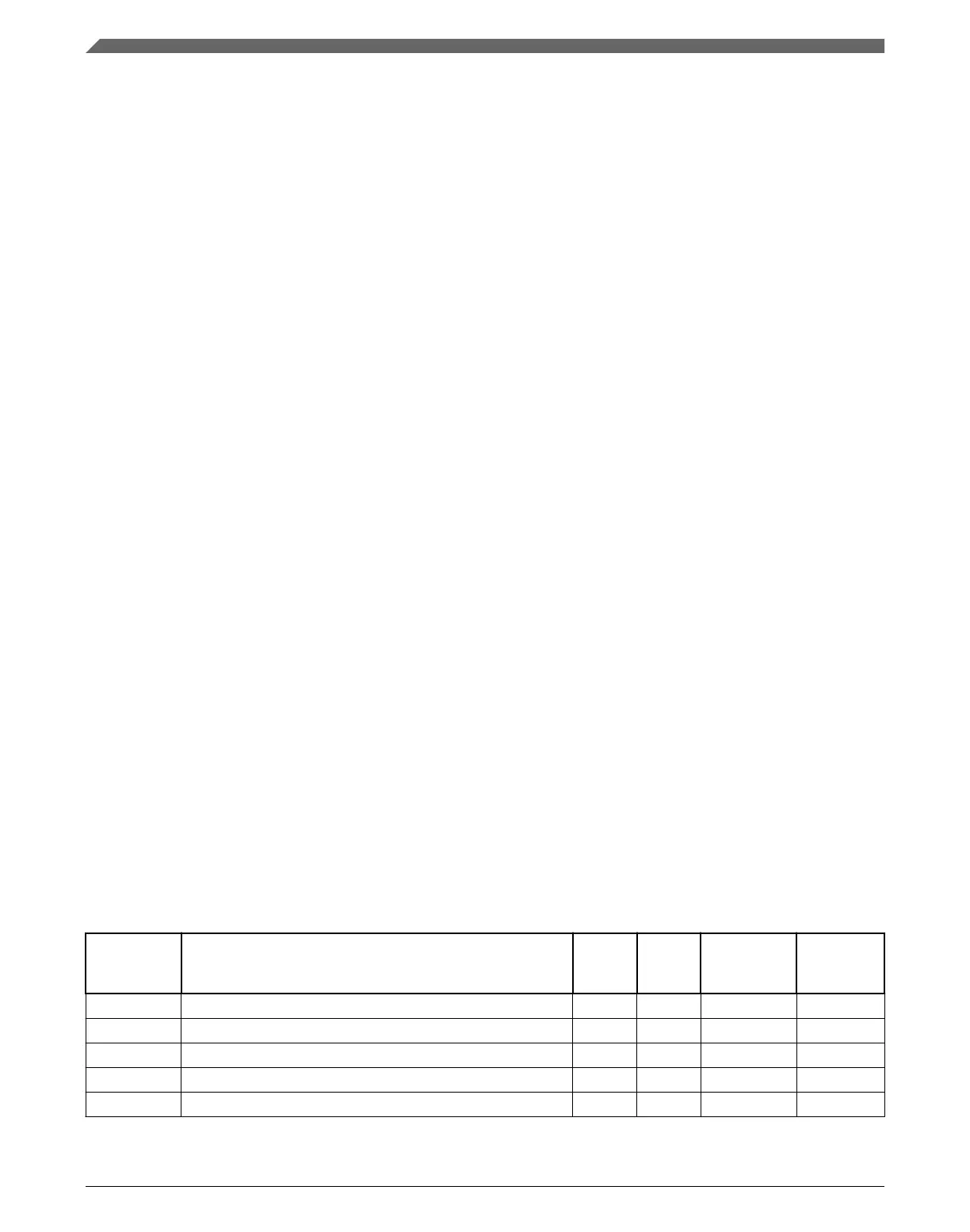
ADC memory map
Absolute
address
(hex)
Register name
Width
(in bits)
Access Reset value
Section/
page
4002_7000 ADC Status and Control Registers 1 (ADC1_SC1A) 32 R/W 0000_001Fh 34.3.1/768
4002_7004 ADC Status and Control Registers 1 (ADC1_SC1B) 32 R/W 0000_001Fh 34.3.1/768
4002_7008 ADC Configuration Register 1 (ADC1_CFG1) 32 R/W 0000_0000h 34.3.2/772
4002_700C ADC Configuration Register 2 (ADC1_CFG2) 32 R/W 0000_0000h 34.3.3/773
4002_7010 ADC Data Result Register (ADC1_RA) 32 R 0000_0000h 34.3.4/774
Table continues on the next page...
Memory map and register definitions
K22F Sub-Family Reference Manual, Rev. 4, 08/2016
766 NXP Semiconductors

 Loading...