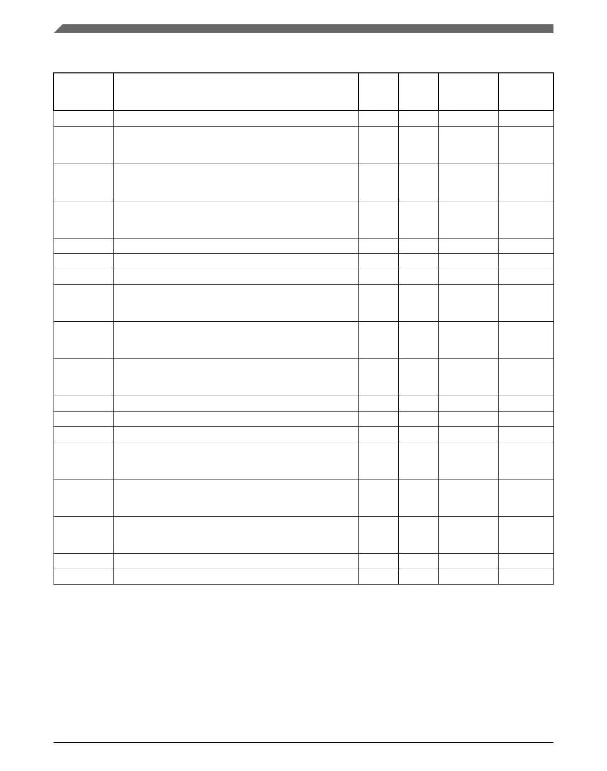
GPIO memory map (continued)
Absolute
address
(hex)
Register name
Width
(in bits)
Access Reset value
Section/
page
400F_F080 Port Data Output Register (GPIOC_PDOR) 32 R/W 0000_0000h 50.2.1/1378
400F_F084 Port Set Output Register (GPIOC_PSOR) 32
W
(always
reads 0)
0000_0000h 50.2.2/1379
400F_F088 Port Clear Output Register (GPIOC_PCOR) 32
W
(always
reads 0)
0000_0000h 50.2.3/1380
400F_F08C Port Toggle Output Register (GPIOC_PTOR) 32
W
(always
reads 0)
0000_0000h 50.2.4/1380
400F_F090 Port Data Input Register (GPIOC_PDIR) 32 R 0000_0000h 50.2.5/1381
400F_F094 Port Data Direction Register (GPIOC_PDDR) 32 R/W 0000_0000h 50.2.6/1381
400F_F0C0 Port Data Output Register (GPIOD_PDOR) 32 R/W 0000_0000h 50.2.1/1378
400F_F0C4 Port Set Output Register (GPIOD_PSOR) 32
W
(always
reads 0)
0000_0000h 50.2.2/1379
400F_F0C8 Port Clear Output Register (GPIOD_PCOR) 32
W
(always
reads 0)
0000_0000h 50.2.3/1380
400F_F0CC Port Toggle Output Register (GPIOD_PTOR) 32
W
(always
reads 0)
0000_0000h 50.2.4/1380
400F_F0D0 Port Data Input Register (GPIOD_PDIR) 32 R 0000_0000h 50.2.5/1381
400F_F0D4 Port Data Direction Register (GPIOD_PDDR) 32 R/W 0000_0000h 50.2.6/1381
400F_F100 Port Data Output Register (GPIOE_PDOR) 32 R/W 0000_0000h 50.2.1/1378
400F_F104 Port Set Output Register (GPIOE_PSOR) 32
W
(always
reads 0)
0000_0000h 50.2.2/1379
400F_F108 Port Clear Output Register (GPIOE_PCOR) 32
W
(always
reads 0)
0000_0000h 50.2.3/1380
400F_F10C Port Toggle Output Register (GPIOE_PTOR) 32
W
(always
reads 0)
0000_0000h 50.2.4/1380
400F_F110 Port Data Input Register (GPIOE_PDIR) 32 R 0000_0000h 50.2.5/1381
400F_F114 Port Data Direction Register (GPIOE_PDDR) 32 R/W 0000_0000h 50.2.6/1381
50.2.1 Port Data Output Register (GPIOx_PDOR)
This register configures the logic levels that are driven on each general-purpose output
pins.
Memory map and register definition
K22F Sub-Family Reference Manual, Rev. 4, 08/2016
1378 NXP Semiconductors

 Loading...