Address
Address Data
TSIZ
AA=1
AA=0
AA=1
AA=0
FB_CLK
FB_RW
FB_TS
FB_ALE
FB_CSn
FB_OEn
FB_BE/BWEn
FB_TA
FB_TSIZ[1:0]
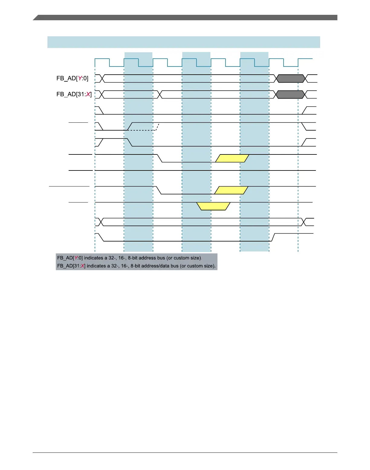
S0 AS WS S2 AHS1 S3 S0
Address Setup Wait State Address Hold
S0 AS WS S2 AHS1 S3 S0
EXTS=0
EXTS=1
Write1WS2AS2AH.svg
Write Cycle with 2-Clock Address Setup and WRAH=1 (1 Wait State)
TIP
Figure 31-21. Write Cycle with Two-Clock Address Setup and Two-Clock Hold (One Wait
State)
31.4.12
Burst cycles
The chip can be programmed to initiate burst cycles if its transfer size exceeds the port
size of the selected destination. The initiation of a burst cycle is encoded on the transfer
size pins (FB_TSIZ[1:0]). For burst transfers to smaller port sizes, FB_TSIZ[1:0]
indicates the size of the entire transfer. For example, with bursting enabled, a 16-bit
transfer to an 8-bit port takes two beats (two byte-sized transfers), for which
FB_TSIZ[1:0] equals 10b throughout. A 32-bit transfer to an 8-bit port takes four beats
(four byte-sized transfers), for which FB_TSIZ[1:0] equals 00b throughout.
Functional description
K22F Sub-Family Reference Manual, Rev. 4, 08/2016
728 NXP Semiconductors
 Loading...

