Device SRAM_L size
(KB)
SRAM_U size
(KB)
Total SRAM (KB) Address Range
MK22FN512VMP12 64 64 128 0x1FFF_0000-0x2000_FFFF
MK22FNX512VFX12 64 64 128 0x1FFF_0000-0x2000_FFFF
MK22FN512CAP12R 64 64 128 0x1FFF_0000-0x2000_FFFF
MK22FN512CBP12R 64 64 128 0x1FFF_0000-0x2000_FFFF
MK22FN256CAP12R 64 64 128 0x1FFF_0000-0x2000_FFFF
3.5.3.2 SRAM retention in low power modes
The SRAM is retained down to LLS3 and VLLS3 mode.
In LLS2 and VLLS2 the 32 KB region of SRAM_U from 0x2000_0000 is powered.
In VLLS1 and VLLS0 no SRAM is retained; however, the 32-byte register file is
available.
3.5.4
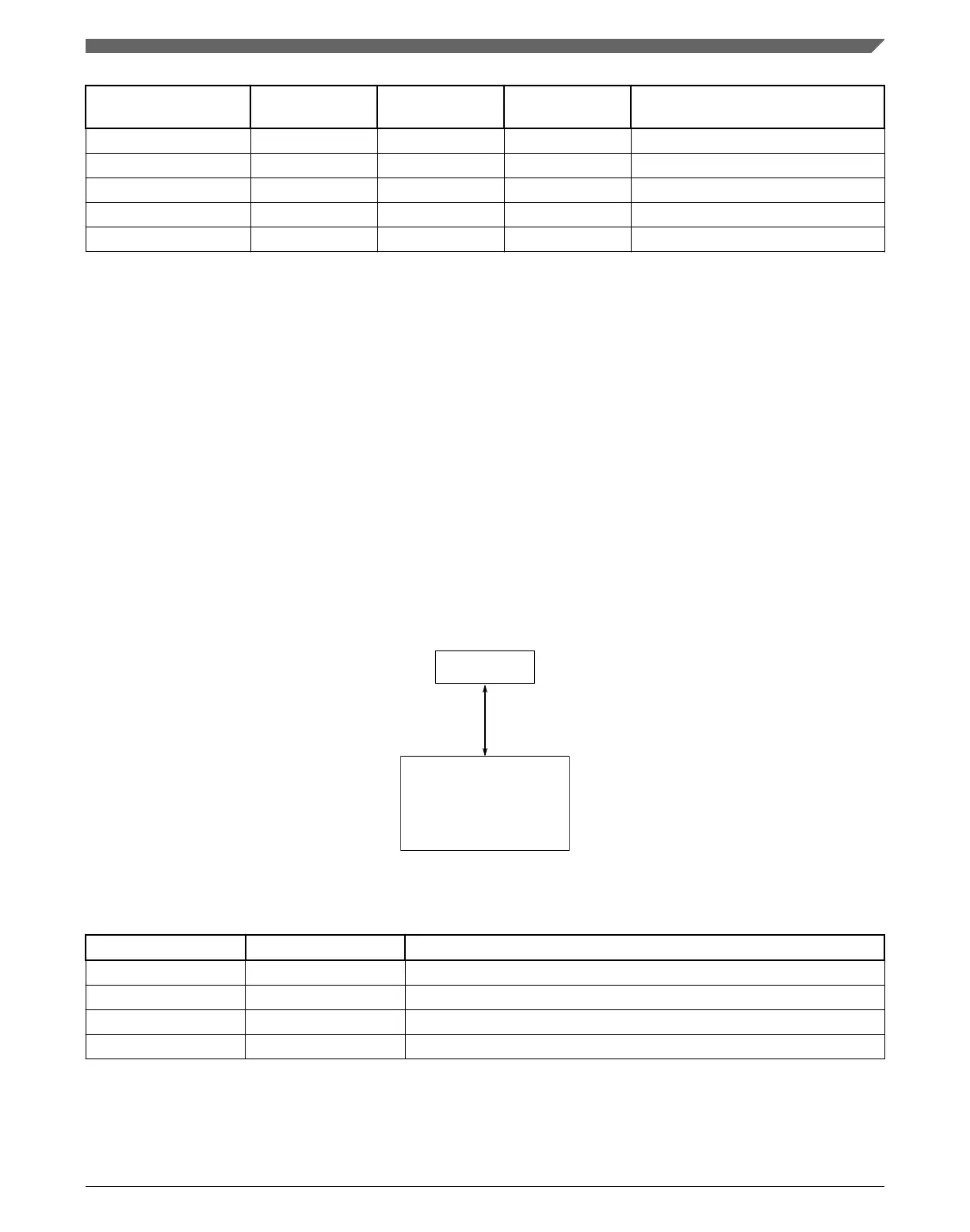
System Register File Configuration
This section summarizes how the module has been configured in the chip.
Register file
Peripheral
bridge 0
Register
access
Figure 3-23. System Register file configuration
Table 3-34. Reference links to related information
Topic Related module Reference
Full description Register file Register file
System memory map System memory map
Clocking Clock distribution
Power management Power management
Chapter 3 Chip Configuration
K22F Sub-Family Reference Manual, Rev. 4, 08/2016
NXP Semiconductors 89

 Loading...