A 32-bit write to the SPI_PUSH register will push all 32-bits to the TX FIFO. An 8-bit or
16-bit write to the 16-bit transmit data field will push the data together with the last
written command word. An 8-bit or 16-bit write to the command word does not push data
onto the FIFO, but that command word is pushed to the TX FIFO on all subsequent 8-bit
or 16-bit writes to the transmit data field. This allows a single 16-bit write to the
command word to be used for all subsequent 8-bit or 16-bit writes to the transmit data
word. Writing a different 16-bit command word will cause all subsequent 8-bit or 16-bit
writes to the transmit data word to be pushed to the TX FIFO with the new command
word.
3.9.3 I2C Configuration
This section summarizes how the module has been configured in the chip. For a
comprehensive description of the module itself, see the module’s dedicated chapter.
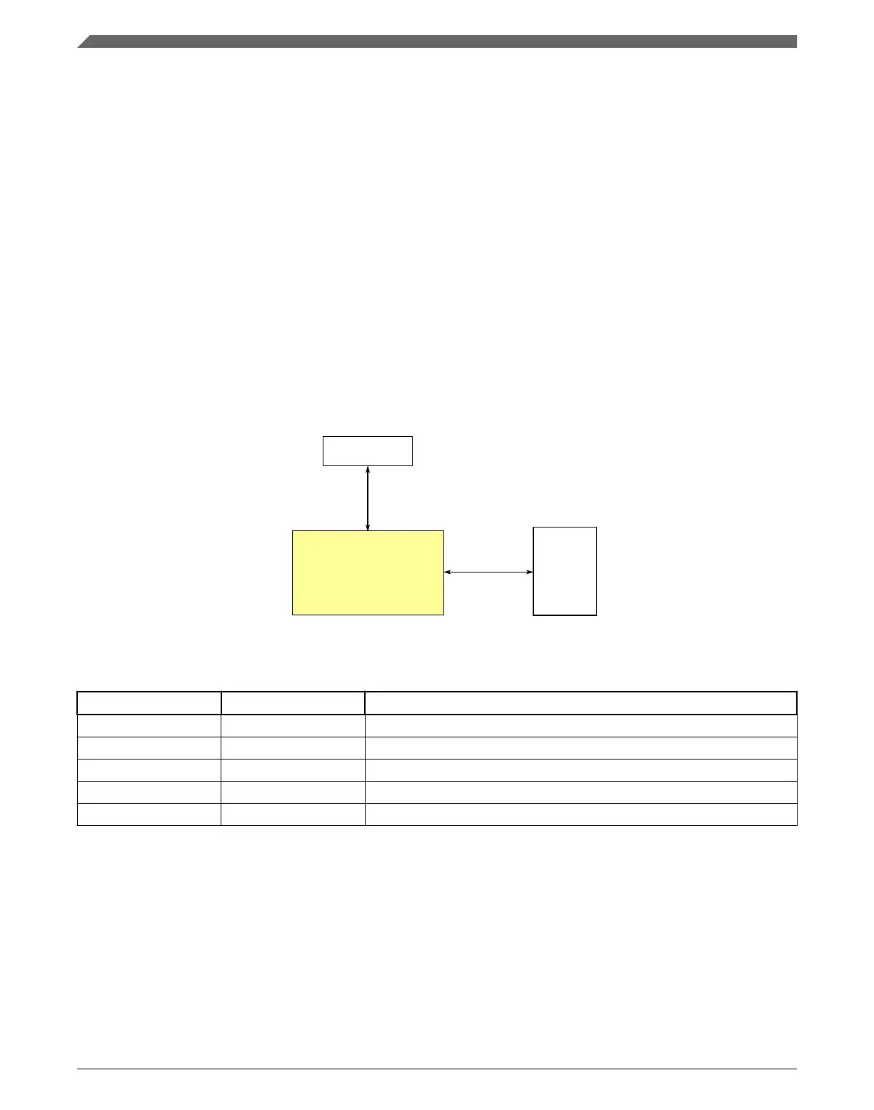
Signal
multiplexing
Register
access
Peripheral
bridge
Module signals
2
I C
Figure 3-53. I2C configuration
Table 3-67. Reference links to related information
Topic Related module Reference
Full description I2C I2C
System memory map System memory map
Clocking Clock Distribution
Power management Power management
Signal Multiplexing Port control Signal Multiplexing
3.9.3.1 I2C Instantiation Information
This device has two I
2
C modules.
The I2C module includes SMBus support and DMA support. It also has optional address
match wakeup in Stop/VLPS mode.
Communication interfaces
K22F Sub-Family Reference Manual, Rev. 4, 08/2016
130 NXP Semiconductors

 Loading...