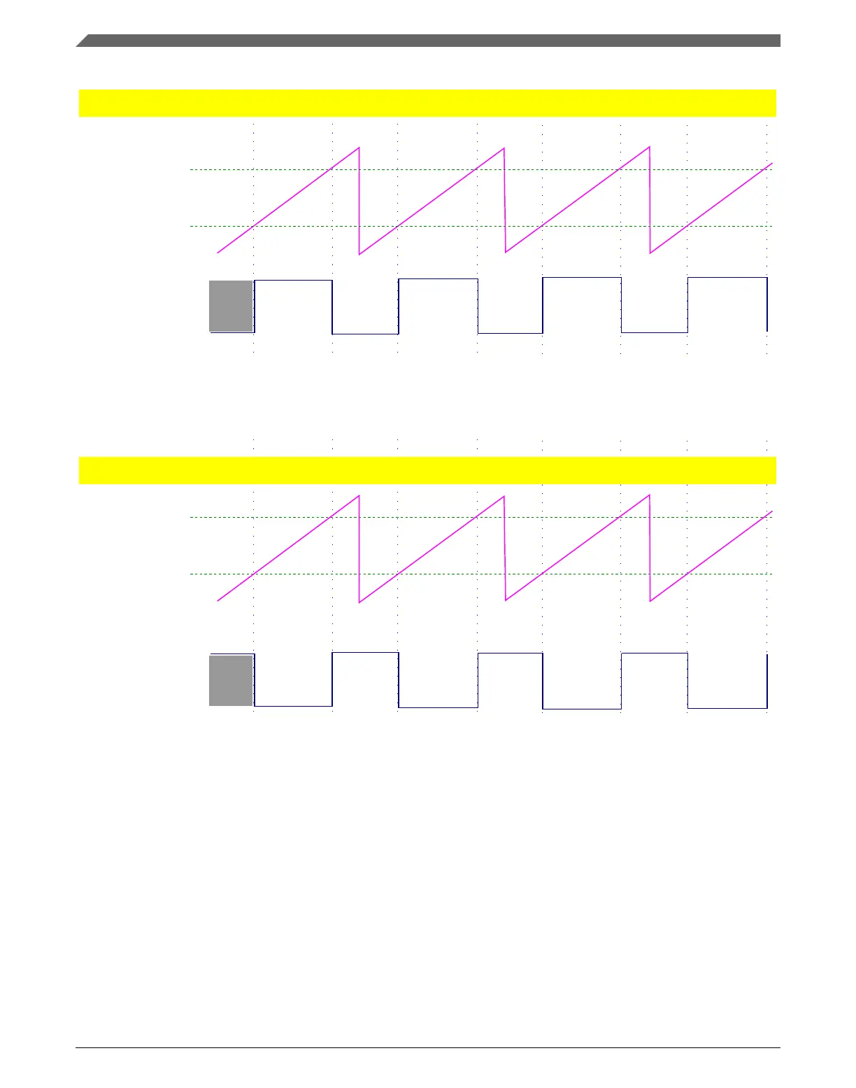
POyDLY[DLY2]
PDB Counter
Pulse-Out
Pulse-Out generation with DLY2 > DLY1
POyDLY[DLY1]
Pulse-Out
Pulse-Out generation with DLY1 > DLY2
POyDLY[DLY1]
PDB Counter
POyDLY[DLY2]
Figure 38-3. How Pulse Out is generated
38.4.4
Updating the delay registers
The following registers control the timing of the PDB operation; and in some of the
applications, they may need to become effective at the same time.
• PDB Modulus register (MOD)
• PDB Interrupt Delay register (IDLY)
•
PDB Channel n Delay m register (CHnDLYm)
Functional description
K22F Sub-Family Reference Manual, Rev. 4, 08/2016
886 NXP Semiconductors

 Loading...