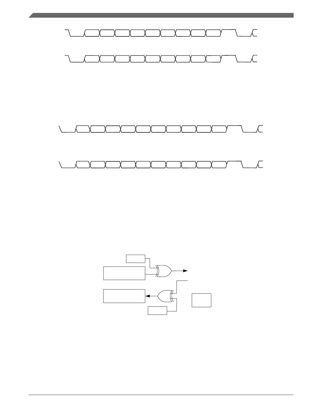
BIT 0 BIT 1 BIT 2 BIT 3 BIT 4 BIT 5 BIT 6 BIT 7
PARITY
STOP
BIT
START
BIT
START
BIT
Figure 47-20. Eight bits of data with LSB first and parity
BIT 7 BIT 6 BIT 5 BIT 4 BIT 3 BIT 2 BIT 1 BIT 0
PARITY
STOP
BIT
START
BIT
START
BIT
Figure 47-21. Eight bits of data with MSB first and parity
47.4.4.3.5 Non-memory mapped tenth bit for parity
The most significant memory-mapped bit can be used for address mark wakeup.
BIT 1 BIT 2 BIT 3 BIT 4 BIT 5 BIT 6 BIT 7 BIT 8
PARITY
STOP
BIT
START
BIT
START
BIT
BIT 0
ADDRESS
MARK
Figure 47-22. Nine bits of data with LSB first and parity
BIT 7 BIT 6 BIT 5 BIT 4 BIT 3 BIT 2 BIT 1 BIT 0
PARITY
STOP
BIT
START
BIT
START
BIT
BIT 8
ADDRESS
MARK
Figure 47-23. Nine bits of data with MSB first and parity
47.4.5
Single-wire operation
Normally, the UART uses two pins for transmitting and receiving. In single wire
operation, the RXD pin is disconnected from the UART and the UART implements a
half-duplex serial connection. The UART uses the TXD pin for both receiving and
transmitting.
RXD
Tx pin input
Tx pin output
TXINV
TRANSMITTER
RECEIVER
RXINV
Figure 47-24. Single-wire operation (C1[LOOPS] = 1, C1[RSRC] = 1)
Enable single wire operation by setting C1[LOOPS] and the receiver source field,
C1[RSRC]. Setting C1[LOOPS] disables the path from the unsynchronized receiver input
signal to the receiver. Setting C1[RSRC] connects the receiver input to the output of the
Functional description
K22F Sub-Family Reference Manual, Rev. 4, 08/2016
1284 NXP Semiconductors

 Loading...