12.2.13 System Clock Divider Register 1 (SIM_CLKDIV1)
When updating CLKDIV1, update all fields using the one write command. Attempting to
write an invalid clock ratio to the CLKDIV1 register will cause the write to be ignored.
The maximum divide ratio that can be programmed between core/system clock and the
other divided clocks is divide by 8. When OUTDIV1 equals 0000 (divide by 1), the other
dividers cannot be set higher than 0111 (divide by 8).
NOTE
The CLKDIV1 register cannot be written to when the device is
in VLPR mode.
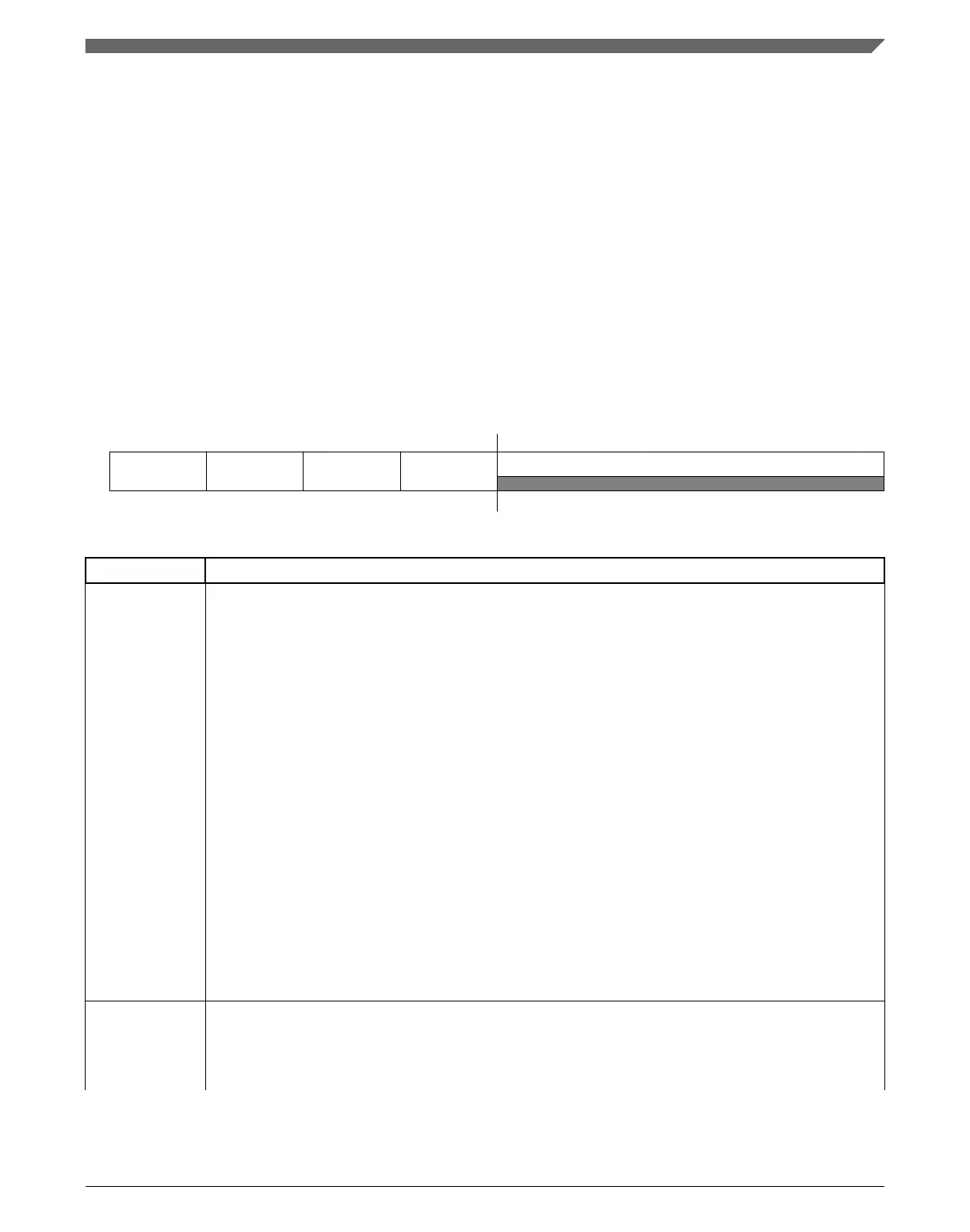
Address:
4004_7000h base + 1044h offset = 4004_8044h
Bit 31 30 29 28 27 26 25 24 23 22 21 20 19 18 17 16 15 14 13 12 11 10 9 8 7 6 5 4 3 2 1 0
R
OUTDIV1 OUTDIV2 OUTDIV3 OUTDIV4
0
W
Reset
0* 0* 0* 0* 0* 0* 0* 0* 0* 0* 0* 0* 0* 0* 0* 1* 0* 0* 0* 0* 0* 0* 0* 0* 0* 0* 0* 0* 0* 0* 0* 0*
SIM_CLKDIV1 field descriptions
Field Description
31–28
OUTDIV1
Clock 1 output divider value
This field sets the divide value for the core/system clock from MCGOUTCLK. At the end of reset, it is
loaded with either 0000 or 0111 depending on FTF_FOPT[LPBOOT].
0000 Divide-by-1.
0001 Divide-by-2.
0010 Divide-by-3.
0011 Divide-by-4.
0100 Divide-by-5.
0101 Divide-by-6.
0110 Divide-by-7.
0111 Divide-by-8.
1000 Divide-by-9.
1001 Divide-by-10.
1010 Divide-by-11.
1011 Divide-by-12.
1100 Divide-by-13.
1101 Divide-by-14.
1110 Divide-by-15.
1111 Divide-by-16.
27–24
OUTDIV2
Clock 2 output divider value
This field sets the divide value for the bus clock from MCGOUTCLK. At the end of reset, it is loaded with
either 0000 or 0111 depending on FTF_FOPT[LPBOOT]. The bus clock frequency must be an integer
divide of the core/system clock frequency.
Table continues on the next page...
Chapter 12 System Integration Module (SIM)
K22F Sub-Family Reference Manual, Rev. 4, 08/2016
NXP Semiconductors 285

 Loading...