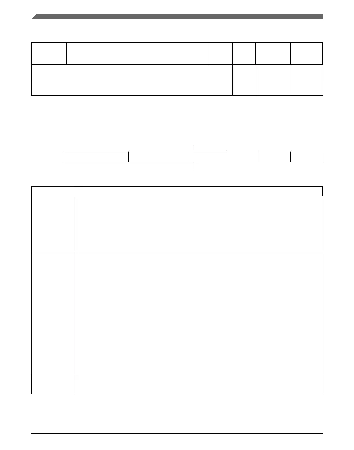
MCG memory map (continued)
Absolute
address
(hex)
Register name
Width
(in bits)
Access Reset value
Section/
page
4006_4012 MCG Status 2 Register (MCG_S2) 8 R/W 00h
25.3.13/
556
4006_4013 MCG Test 3 Register (MCG_T3) 8 R/W 00h
25.3.13/
557
25.3.1 MCG Control 1 Register (MCG_C1)
Address: 4006_4000h base + 0h offset = 4006_4000h
Bit 7 6 5 4 3 2 1 0
Read
CLKS FRDIV IREFS IRCLKEN IREFSTEN
Write
Reset
0 0 0 0 0 1 0 0
MCG_C1 field descriptions
Field Description
7–6
CLKS
Clock Source Select
Selects the clock source for MCGOUTCLK .
00 Encoding 0 — Output of FLL or PLL is selected (depends on PLLS control bit).
01 Encoding 1 — Internal reference clock is selected.
10 Encoding 2 — External reference clock is selected.
11 Encoding 3 — Reserved.
5–3
FRDIV
FLL External Reference Divider
Selects the amount to divide down the external reference clock for the FLL. The resulting frequency must
be in the range 31.25 kHz to 39.0625 kHz (This is required when FLL/DCO is the clock source for
MCGOUTCLK . In FBE mode, it is not required to meet this range, but it is recommended in the cases
when trying to enter a FLL mode from FBE).
000 If RANGE = 0 or OSCSEL=1 , Divide Factor is 1; for all other RANGE values, Divide Factor is 32.
001 If RANGE = 0 or OSCSEL=1 , Divide Factor is 2; for all other RANGE values, Divide Factor is 64.
010 If RANGE = 0 or OSCSEL=1 , Divide Factor is 4; for all other RANGE values, Divide Factor is 128.
011 If RANGE = 0 or OSCSEL=1 , Divide Factor is 8; for all other RANGE values, Divide Factor is 256.
100 If RANGE = 0 or OSCSEL=1 , Divide Factor is 16; for all other RANGE values, Divide Factor is 512.
101 If RANGE = 0 or OSCSEL=1 , Divide Factor is 32; for all other RANGE values, Divide Factor is
1024.
110 If RANGE = 0 or OSCSEL=1 , Divide Factor is 64; for all other RANGE values, Divide Factor is
1280 .
111 If RANGE = 0 or OSCSEL=1 , Divide Factor is 128; for all other RANGE values, Divide Factor is
1536 .
2
IREFS
Internal Reference Select
Selects the reference clock source for the FLL.
Table continues on the next page...
Memory Map/Register Definition
K22F Sub-Family Reference Manual, Rev. 4, 08/2016
544 NXP Semiconductors
 Loading...

