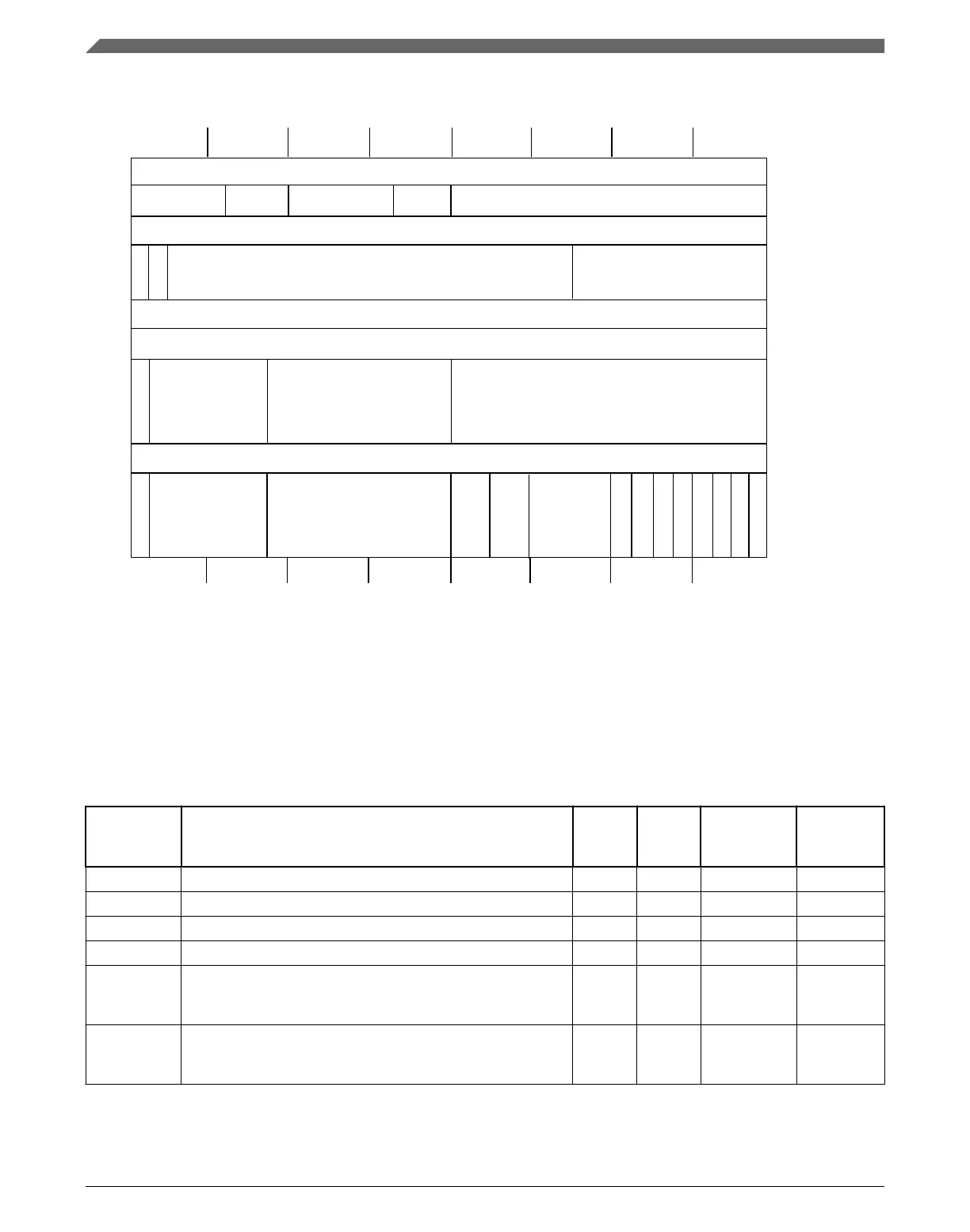
22.3.3 TCD structure
SADDR
31 30
29
28
27
26
25
24
23
22 21
20
19
18
17
16
15
14
13
12
11
10 9
8
7
6
5 4
3
2
1
0
SOFFSMOD SSIZE
DMOD
DSIZE
SMLOE
DMLOE
MLOFF or NBYTES NBYTES
SLAST
DADDR
31 30
29
28
27
26
25
24
23
22 21
20
19
18
17
16
15
14
13
12
11
10 9
8
7
6
5 4
3
2
1
0
CITER.E_LINK
CITER or
CITER.LINKCH
CITER
DOFF
DLAST_SGA
BITER.E_LINK
BITER or
BITER.LINKCH
BITER
START
INT_MAJ
INT_HALF
D_REQ
E_SG
MAJOR.E_LINK
ACTIVE
DONE
BWC
MAJOR.LINKCH
NBYTES
0000h
0004h
0008h
DMA_CR[EMLM] enabled
000Ch
0010h
0014h
0018h
001Ch
Reserved
DMA_CR[EMLM] disabled
{
{
{
22.3.4 Reserved memory and bit fields
• Reading reserved bits in a register returns the value of zero.
• Writes to reserved bits in a register are ignored.
• Reading or writing a reserved memory location generates a bus error.
DMA memory map
Absolute
address
(hex)
Register name
Width
(in bits)
Access Reset value
Section/
page
4000_8000 Control Register (DMA_CR) 32 R/W 0000_0000h 22.3.5/441
4000_8004 Error Status Register (DMA_ES) 32 R 0000_0000h 22.3.6/444
4000_800C Enable Request Register (DMA_ERQ) 32 R/W 0000_0000h 22.3.7/446
4000_8014 Enable Error Interrupt Register (DMA_EEI) 32 R/W 0000_0000h 22.3.8/448
4000_8018 Clear Enable Error Interrupt Register (DMA_CEEI) 8
W
(always
reads 0)
00h 22.3.9/450
4000_8019 Set Enable Error Interrupt Register (DMA_SEEI) 8
W
(always
reads 0)
00h 22.3.10/451
Table continues on the next page...
Memory map/register definition
K22F Sub-Family Reference Manual, Rev. 4, 08/2016
430 NXP Semiconductors

 Loading...