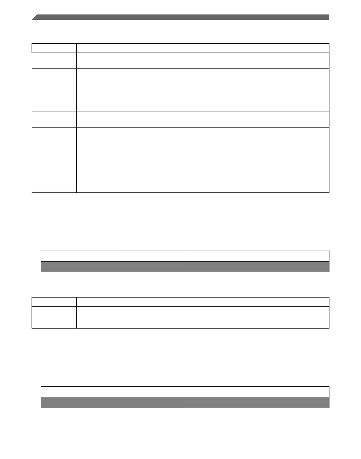
SIM_FCFG2 field descriptions
Field Description
31
Reserved
This field is reserved.
This read-only field is reserved and always has the value 0.
30–24
MAXADDR0
Max address block 0
This field concatenated with 13 trailing zeros indicates the first invalid address of each program flash
block.
For example, if MAXADDR0 = 0x20 the first invalid address of flash block 0 is 0x0004_0000. This would
be the MAXADDR0 value for a device with 256 KB program flash in flash block 0.
23
Reserved
This field is reserved.
This read-only field is reserved and always has the value 1.
22–16
MAXADDR1
Max address block 1
This field equals zero if there is only one program flash block, otherwise it equals the value of the
MAXADDR0 field.
For example, with MAXADDR0 = MAXADDR1 = 0x20 the first invalid address of flash block 1 is 0x4_0000
+ 0x4_0000. This would be the MAXADDR1 value for a device with 512 KB program flash memory across
two flash blocks and no FlexNVM.
Reserved This field is reserved.
This read-only field is reserved and always has the value 0.
12.2.17 Unique Identification Register High (SIM_UIDH)
Address: 4004_7000h base + 1054h offset = 4004_8054h
Bit 31 30 29 28 27 26 25 24 23 22 21 20 19 18 17 16 15 14 13 12 11 10 9 8 7 6 5 4 3 2 1 0
R
UID
W
Reset
0* 0* 0* 0* 0* 0* 0* 0* 0* 0* 0* 0* 0* 0* 0* 0* 0* 0* 0* 0* 0* 0* 0* 0* 0* 0* 0* 0* 0* 0* 0* 0*
SIM_UIDH field descriptions
Field Description
UID Unique Identification
Unique identification for the device.
12.2.18 Unique Identification Register Mid-High (SIM_UIDMH)
Address: 4004_7000h base + 1058h offset = 4004_8058h
Bit 31 30 29 28 27 26 25 24 23 22 21 20 19 18 17 16 15 14 13 12 11 10 9 8 7 6 5 4 3 2 1 0
R
UID
W
Reset
0* 0* 0* 0* 0* 0* 0* 0* 0* 0* 0* 0* 0* 0* 0* 0* 0* 0* 0* 0* 0* 0* 0* 0* 0* 0* 0* 0* 0* 0* 0* 0*
Memory map and register definition
K22F Sub-Family Reference Manual, Rev. 4, 08/2016
290 NXP Semiconductors

 Loading...