51.3.3 Device identification register
The device identification (JTAG ID) register, shown in the following figure, allows the
revision number, part number, manufacturer, and design center responsible for the design
of the part to be determined through the TAP. The device identification register is
selected for serial data transfer between TDI and TDO when the IDCODE instruction is
active. Entry into the Capture-DR state while the device identification register is selected
loads the IDCODE into the shift register to be shifted out on TDO in the Shift-DR state.
No action occurs in the Update-DR state.
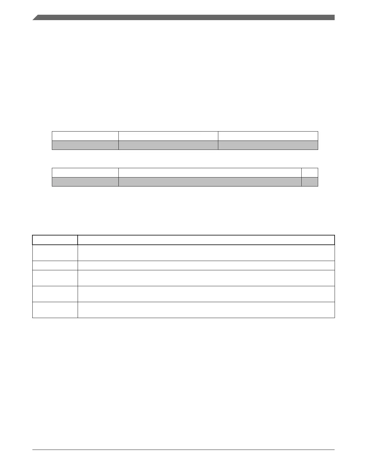
31 30 29 28 27 26 25 24 23 22 21 20 19 18 17 16
R Part Revision Number Design Center Part Identification Number
W
Reset
PRN DC PIN
15 14 13 12 11 10 9 8 7 6 5 4 3 2 1 0
R Part Identification Number Manufacturer Identity Code 1
W
Reset
PIN (contd.) MIC 1
The following table describes the device identification register functions.
Table 51-2. Device identification register field descriptions
Field Description
PRN Part Revision Number. Contains the revision number of the part. Value is On this device, the PIN mirrors
bits 9-0 of the SIM_SDID[REVID] field. Please see the SIM_SDID register description for more detail.
DC Design Center. Indicates the design center. Value is 0x2C.
PIN Part Identification Number. Contains the part number of the device. On this device, the PIN mirrors bits 9-0
of the SIM_SDID register. Please see the SIM_SDID register description for more detail.
MIC Manufacturer Identity Code. Contains the reduced Joint Electron Device Engineering Council (JEDEC) ID.
Value is 0x00E.
IDCODE ID IDCODE Register ID. Identifies this register as the device identification register and not the bypass
register. Always set to 1.
51.3.4 Boundary scan register
The boundary scan register is connected between TDI and TDO when the EXTEST,
SAMPLE or SAMPLE/PRELOAD instructions are active. It is used to capture input pin
data, force fixed values on output pins, and select a logic value and direction for
bidirectional pins. Each bit of the boundary scan register represents a separate boundary
scan register cell, as described in the IEEE 1149.1-2001 standard and discussed in
Boundary scan. The size of the boundary scan register and bit ordering is device-
dependent and can be found in the device BSDL file.
Register description
K22F Sub-Family Reference Manual, Rev. 4, 08/2016
1388 NXP Semiconductors

 Loading...