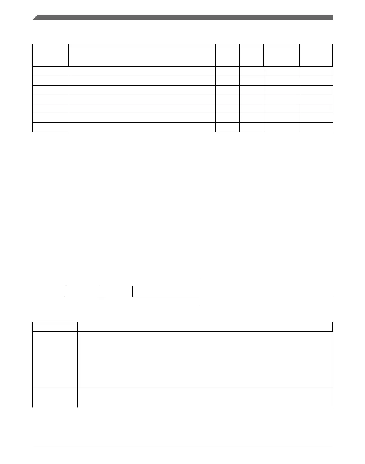
DMAMUX memory map (continued)
Absolute
address
(hex)
Register name
Width
(in bits)
Access Reset value
Section/
page
4002_1009 Channel Configuration register (DMAMUX_CHCFG10) 8 R/W 00h 21.3.1/416
4002_100A Channel Configuration register (DMAMUX_CHCFG9) 8 R/W 00h 21.3.1/416
4002_100B Channel Configuration register (DMAMUX_CHCFG8) 8 R/W 00h 21.3.1/416
4002_100C Channel Configuration register (DMAMUX_CHCFG15) 8 R/W 00h 21.3.1/416
4002_100D Channel Configuration register (DMAMUX_CHCFG14) 8 R/W 00h 21.3.1/416
4002_100E Channel Configuration register (DMAMUX_CHCFG13) 8 R/W 00h 21.3.1/416
4002_100F Channel Configuration register (DMAMUX_CHCFG12) 8 R/W 00h 21.3.1/416
21.3.1 Channel Configuration register (DMAMUX_CHCFGn)
Each of the DMA channels can be independently enabled/disabled and associated with
one of the DMA slots (peripheral slots or always-on slots) in the system.
NOTE
Setting multiple CHCFG registers with the same source value
will result in unpredictable behavior. This is true, even if a
channel is disabled (ENBL==0).
Before changing the trigger or source settings, a DMA channel
must be disabled via CHCFGn[ENBL].
Address:
4002_1000h base + 0h offset + (1d × i), where i=0d to 15d
Bit 7 6 5 4 3 2 1 0
Read
ENBL TRIG SOURCE
Write
Reset
0 0 0 0 0 0 0 0
DMAMUX_CHCFGn field descriptions
Field Description
7
ENBL
DMA Channel Enable
Enables the DMA channel.
0 DMA channel is disabled. This mode is primarily used during configuration of the DMAMux. The DMA
has separate channel enables/disables, which should be used to disable or reconfigure a DMA
channel.
1 DMA channel is enabled
6
TRIG
DMA Channel Trigger Enable
Enables the periodic trigger capability for the triggered DMA channel.
Table continues on the next page...
Memory map/register definition
K22F Sub-Family Reference Manual, Rev. 4, 08/2016
416 NXP Semiconductors

 Loading...