51.2 External signal description
The JTAGC consists of a set of signals that connect to off chip development tools and
allow access to test support functions. The JTAGC signals are outlined in the following
table and described in the following sections.
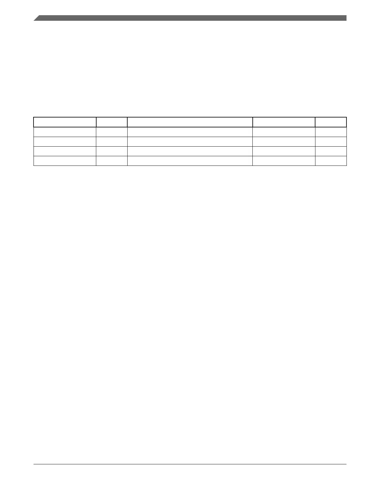
Table 51-1. JTAG signal properties
Name I/O Function Reset State Pull
TCK Input Test Clock — Down
TDI Input Test Data In — Up
TDO Output Test Data Out High Z
1
—
TMS Input Test Mode Select — Up
1. TDO output buffer enable is negated when the JTAGC is not in the Shift-IR or Shift-DR states. A weak pull may be
implemented at the TDO pad for use when JTAGC is inactive.
51.2.1 TCK—Test clock input
Test Clock Input (TCK) is an input pin used to synchronize the test logic and control
register access through the TAP.
51.2.2
TDI—Test data input
Test Data Input (TDI) is an input pin that receives serial test instructions and data. TDI is
sampled on the rising edge of TCK.
51.2.3
TDO—Test data output
Test Data Output (TDO) is an output pin that transmits serial output for test instructions
and data. TDO is three-stateable and is actively driven only in the Shift-IR and Shift-DR
states of the TAP controller state machine, which is described in TAP controller state
machine.
51.2.4
TMS—Test mode select
Test Mode Select (TMS) is an input pin used to sequence the IEEE 1149.1-2001 test
control state machine. TMS is sampled on the rising edge of TCK.
External signal description
K22F Sub-Family Reference Manual, Rev. 4, 08/2016
1386 NXP Semiconductors

 Loading...