35.7 Digital-to-analog converter
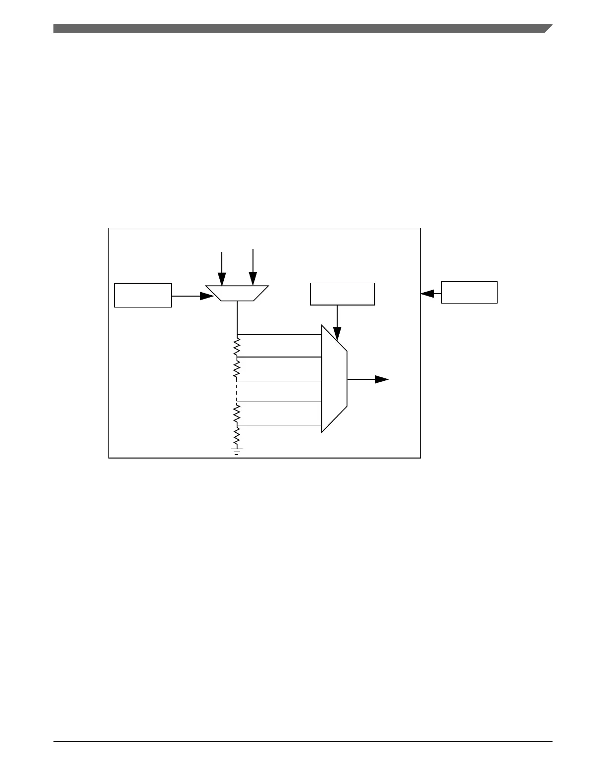
The figure found here shows the block diagram of the DAC module.
It contains a 64-tap resistor ladder network and a 64-to-1 multiplexer, which selects an
output voltage from one of 64 distinct levels that outputs from DACO. It is controlled
through the DAC Control Register (DACCR). Its supply reference source can be selected
from two sources V
in1
and V
in2
. The module can be powered down or disabled when not
in use. When in Disabled mode, DACO is connected to the analog ground.
VOSEL[5:0]
DACO
MUX
MUX
DACEN
Vin
VRSEL
Vin1
Vin2
Figure 35-12. 6-bit DAC block diagram
35.8
DAC functional description
This section provides DAC functional description information.
35.8.1
Voltage reference source select
• V
in1
connects to the primary voltage source as supply reference of 64 tap resistor
ladder
• V
in2
connects to an alternate voltage source
Chapter 35 Comparator (CMP)
K22F Sub-Family Reference Manual, Rev. 4, 08/2016
NXP Semiconductors 843

 Loading...